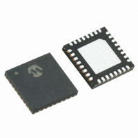
MRF89XA-I/MQ Microchip Technology, MRF89XA-I/MQ Datasheet - Page 17

MRF89XA-I/MQ
Manufacturer Part Number
MRF89XA-I/MQ
Description
TXRX ISM SUB-GHZ ULP 32QFN
Manufacturer
Microchip Technology
Specifications of MRF89XA-I/MQ
Package / Case
32-WFQFN Exposed Pad
Frequency
863MHz ~ 870MHz, 902MHz ~ 928MHz, 950MHz ~ 960MHz
Data Rate - Maximum
200kbps
Modulation Or Protocol
FSK, OOK
Applications
ISM
Power - Output
12.5dBm
Sensitivity
-113dBm
Voltage - Supply
2.1 V ~ 3.6 V
Current - Receiving
3mA
Current - Transmitting
25mA
Data Interface
PCB, Surface Mount
Antenna Connector
PCB, Surface Mount
Operating Temperature
-40°C ~ 85°C
Number Of Receivers
1
Number Of Transmitters
1
Wireless Frequency
863 MHz to 870 MHz, 902 MHz to 928 MHz, 950 MHz to 960 MHz
Interface Type
SPI
Noise Figure
- 112 dBc
Output Power
- 8.5 dBm, + 12.5 dBm
Operating Supply Voltage
2.1 V to 3.6 V
Maximum Operating Temperature
+ 85 C
Mounting Style
SMD/SMT
Maximum Data Rate
256 Kbps
Maximum Supply Current
25 mA
Minimum Operating Temperature
- 40 C
Modulation
FSK
Lead Free Status / RoHS Status
Lead free / RoHS Compliant
Memory Size
-
Lead Free Status / Rohs Status
Lead free / RoHS Compliant
Available stocks
Company
Part Number
Manufacturer
Quantity
Price
Company:
Part Number:
MRF89XA-I/MQ
Manufacturer:
MICROCHIP
Quantity:
12 000
2.5.2
The transceiver can provide a clock signal through the
CLKOUT pin (pin 19) to the microcontroller for accurate
timing, thereby eliminating the need for a second
The CLKOUT is a sub-multiple of the reference
frequency and is programmable.
The two main functions of the CLKOUT output are:
• To
• To
CLKOUT can be made available in any operation
mode, except Sleep mode, and is automatically
enabled at power-up.
2.5.3
The Integer-N Phase-Locked Loop (PLL) circuitry
determines the operating frequency of the device. The
PLL maintains accuracy by using the crystal-controlled
reference oscillator and provides maximum flexibility in
performance to the designers.
The high resolution of the PLL allows the use of
multiple channels in any of the bands. The on-chip PLL
is capable of performing manual and automatic
calibration to compensate for the changes in
temperature or operating voltage.
FIGURE 2-5:
© 2010 Microchip Technology Inc.
crystal. This results in reducing the component count.
microcontroller, thus saving the cost of an
additional oscillator.
Measurement of the CLKOUT signal enables
simple software trimming of the initial crystal
tolerance.
Note:
provide
provide
VCO Output
CLKOUT OUTPUT PIN (CLKOUT)
To minimize the current consumption of
the MRF89XA, ensure that the CLKOUT
signal is disabled when unused.
PHASE-LOCKED LOOP
ARCHITECTURE
LO
an
a
clock
oscillator
LO VCO OUTPUT GENERATOR
output
reference
for
÷8
÷8
a
output.
host
Preliminary
2.5.3.1
The MRF89XA features a PLL lock detect indicator
(PLOCK). This is useful for optimizing power consump-
tion, by adjusting the synthesizer wake-up time. The
lock status can also be read on the LSTSPLL bit from
the FTPRIREG register (Register 2-15), and must be
cleared by writing a ‘1’ to this same register. The lock
status is available on the PLOCK pin (pin 23), by setting
the LENPLL bit in the FTPRIREG register.
2.5.4
The integrated Voltage Controlled Oscillator (VCO)
requires two external tank circuit inductors. As the input
is differential, the two inductors should have the same
nominal value. The performance of these components
are essential for both the phase noise and the power
consumption of the PLL. It is recommended that a pair
of high Q inductors is selected. These should be
mounted orthogonally to other inductors in the circuit
(in particular the PA choke) to reduce spurious coupling
between the PA and VCO. For best performance, wire
wound high-Q inductors with tight tolerance should be
used as described in Section 4.0 “Application
Details”. In addition, such measures may reduce radi-
ated pulling effects and undesirable transient behavior,
thus minimizing spectral occupancy.
The output signal of the VCO is used as the input to the
local oscillator (LO) generator stage, as illustrated in
Figure 2-5.The VCO frequency is subdivided and used
in a series of up (down) conversions for transmission
(reception).
90º
90º
90º
Note:
VOLTAGE CONTROLLED
OSCILLATOR
Ensuring a symmetrical layout of the VCO
inductors will further improve PLL spectral
purity.
PLL Lock Pin (PLOCK)
Q
Q
I
I
Q
I
LO1 RX
LO2 RX
LO1 TX
LO2 TX
MRF89XA
Receiver
LOs
Transmitter
LOs
DS70622B-page 17


