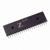
Z85C3010PSG Zilog, Z85C3010PSG Datasheet - Page 195

Z85C3010PSG
Manufacturer Part Number
Z85C3010PSG
Description
IC 10MHZ Z8500 CMOS SCC 40-DIP
Manufacturer
Zilog
Series
SCCr
Specifications of Z85C3010PSG
Processor Type
Z80
Features
Error Detection and Multiprotocol Support
Speed
10MHz
Voltage
5V
Mounting Type
Through Hole
Package / Case
40-DIP (0.620", 15.75mm)
Cpu Speed
8MHz
Digital Ic Case Style
DIP
No. Of Pins
40
Supply Voltage Range
5V
Operating Temperature Range
0°C To +70°C
Svhc
No SVHC (18-Jun-2010)
Base Number
85
Rohs Compliant
Yes
Clock Frequency
10MHz
Lead Free Status / RoHS Status
Lead free / RoHS Compliant
Other names
269-3934
Z85C3010PSG
Z85C3010PSG
Available stocks
Company
Part Number
Manufacturer
Quantity
Price
Company:
Part Number:
Z85C3010PSG
Manufacturer:
Zilog
Quantity:
135
Company:
Part Number:
Z85C3010PSG
Manufacturer:
Zilog
Quantity:
326
- Current page: 195 of 317
- Download datasheet (4Mb)
Application Note
The Zilog Datacom Family with the 80186 CPU
Processor
The 80186 may be operated at rates up to 16 MHz. To use
the CPU clock for accurate serial bit clocking, a 9.8304
MHz CPU clock can be used. The crystal connected to the
processor is 2X the operating frequency.
The processor’s 1 Mbyte address space is well filled if the
maximum RAM complement is installed. Of the integrated
Chip Select outputs provided by the 80186, the /UCS
output is used for the EPROMs, and all of the /PCS6-
/PCS0 outputs are used for the datacom controllers. A
hardware address decoder is used for the SRAMs instead
of the 80186’s /LCS and /MCS3-/MCS0 outputs because
the RAMs must be accessible to the on-chip DMA
functions of the ISCC and IUSC as well as the 80186. The
80186 does not decode addresses from external bus
masters. Both 8-bit and 16-bit accesses are provided for
RAM. The EPROMs are only accessible to the 80186.
If more than one channel among the ESCC B and (M)USC
are enabled for one of the 80186’s internal DMA channels,
software must ensure that only one of the enabled devices
makes requests during a given block transfer. This can be
done by leaving an entire Receiver or Transmitter idle or
disabled, or by programming the device so that the DMA
request is not output on the pin.
The ISCC and IUSC handle their own DMA transfers via
the 80186’s HOLD/HLDA facility.
Note: Either a Z16C33 MUSC or a Z16C30 USC can be
installed in socket U5. If this is done, references to the
(M)USC herein after may mean the USC as a whole or just
its channel A; which one should be clear from the context.
The inputs and outputs associated with the processor’s
integrated counter/timer facility are brought to the pin
6-60
GENERAL DESCRIPTION (Continued)
To enable the following to use 80186 DMA Channel 0:
(E)SCC B Rx
MUSC Rx or USC A Rx
MUSC Tx or USC A Tx
USC B Rx
USC B Tx
To enable the following to use 80186 DMA Channel 1:
ESCC B Tx
(E)SCC B Tx w/early release
MUSC Rx or USC A Rx
MUSC Tx or USC A Tx
USC B Rx
USC B Tx
Table 1. 80186 DMA Jumper Connections
The 80186’s mid-range memory chip select feature
(specifically, the /MCS2 output) is used to give the
software a way to hardware Reset the ISCC, IUSC, and
(M)USC. This allows a customer’s program to operate as
if it were in a target system starting from Reset, including
the initial write to the Bus Configuration Register (BCR).
The 80186’s two integrated DMA channels can be used for
any two of the four or six serial data streams in the B side
of the (E)SCC and the (M)USC. The “DMA EPLD” derives
requests for the 80186’s two DMA channels from six
inputs, two each for (E)SCC channel B and the one or two
channels in the (M)USC. It asserts DREQ0 or DREQ1
(High) if any of the inputs for that channel is low, and the
80186 is not performing an Interrupt Acknowledge cycle.
Jumper blocks J22, J23, J24, and J29 control the
assignment of the 80186’s internal DMA controllers,
including provision for a clipped Tx request that is needed
if a standard SCC is installed in place of the ESCC. The
various possibilities are summarized in Table 1.
header labelled J26 so that they can be used in
applications (Table 2).
The 80186’s integrated interrupt controller is largely
bypassed in favor of the traditional Zilogical interrupt
daisy-chain structure.
J26 pin
1
2
3
4
5
6
Table 2. Counter/Timer Signal Locations
Install this jumper:
J23-1 to J23-2
J22-1 to J22-2
J22-4 to J22-2
J29-1 to J29-2
J29-4 to J29-2
Install this Jumper:
J24-1 to J24-3
J24-1 to J24-2
J22-1 to J22-3
J22-4 to J22-3
J29-1 to J29-3
J29-4 to J29-3
Signal
Timer In 1
Timer Out 1
Timer In 0
Timer Out 0
N/C
Ground
UM010901-0601
Related parts for Z85C3010PSG
Image
Part Number
Description
Manufacturer
Datasheet
Request
R

Part Number:
Description:
Manufacturer:
Zilog, Inc.
Datasheet:

Part Number:
Description:
Cmos Scc Serial Communications Controller
Manufacturer:
ZiLOG Semiconductor
Datasheet:

Part Number:
Description:
Communication Controllers, ZILOG INTELLIGENT PERIPHERAL CONTROLLER (ZIP)
Manufacturer:
Zilog, Inc.
Datasheet:

Part Number:
Description:
KIT DEV FOR Z8 ENCORE 16K TO 64K
Manufacturer:
Zilog
Datasheet:

Part Number:
Description:
KIT DEV Z8 ENCORE XP 28-PIN
Manufacturer:
Zilog
Datasheet:

Part Number:
Description:
DEV KIT FOR Z8 ENCORE 8K/4K
Manufacturer:
Zilog
Datasheet:

Part Number:
Description:
KIT DEV Z8 ENCORE XP 28-PIN
Manufacturer:
Zilog
Datasheet:

Part Number:
Description:
DEV KIT FOR Z8 ENCORE 4K TO 8K
Manufacturer:
Zilog
Datasheet:

Part Number:
Description:
CMOS Z8 microcontroller. ROM 16 Kbytes, RAM 256 bytes, speed 16 MHz, 32 lines I/O, 3.0V to 5.5V
Manufacturer:
Zilog, Inc.
Datasheet:

Part Number:
Description:
Low-cost microcontroller. 512 bytes ROM, 61 bytes RAM, 8 MHz
Manufacturer:
Zilog, Inc.
Datasheet:

Part Number:
Description:
Z8 4K OTP Microcontroller
Manufacturer:
Zilog, Inc.
Datasheet:

Part Number:
Description:
CMOS SUPER8 ROMLESS MCU
Manufacturer:
Zilog, Inc.
Datasheet:

Part Number:
Description:
SL1866 CMOSZ8 OTP Microcontroller
Manufacturer:
Zilog, Inc.
Datasheet:


