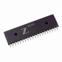
Z85C3010PSG Zilog, Z85C3010PSG Datasheet - Page 36

Z85C3010PSG
Manufacturer Part Number
Z85C3010PSG
Description
IC 10MHZ Z8500 CMOS SCC 40-DIP
Manufacturer
Zilog
Series
SCCr
Specifications of Z85C3010PSG
Processor Type
Z80
Features
Error Detection and Multiprotocol Support
Speed
10MHz
Voltage
5V
Mounting Type
Through Hole
Package / Case
40-DIP (0.620", 15.75mm)
Cpu Speed
8MHz
Digital Ic Case Style
DIP
No. Of Pins
40
Supply Voltage Range
5V
Operating Temperature Range
0°C To +70°C
Svhc
No SVHC (18-Jun-2010)
Base Number
85
Rohs Compliant
Yes
Clock Frequency
10MHz
Lead Free Status / RoHS Status
Lead free / RoHS Compliant
Other names
269-3934
Z85C3010PSG
Z85C3010PSG
Available stocks
Company
Part Number
Manufacturer
Quantity
Price
Company:
Part Number:
Z85C3010PSG
Manufacturer:
Zilog
Quantity:
135
Company:
Part Number:
Z85C3010PSG
Manufacturer:
Zilog
Quantity:
326
- Current page: 36 of 317
- Download datasheet (4Mb)
UM010901-0601
ESCC:
The receive interrupt request is either caused by a re-
ceive character available or a special condition. When
the receive character available interrupt is generated,
it is dependent on WR7' bit D3. If WR7' D3=0, the re-
ceive character available interrupt is generated when
one character is loaded into the FIFO and is ready to
be read. If WR7' D3=1, the receive character available
interrupt is generated when four bytes are available to
be read in the receive data FIFO. The programmed val-
ue of WR7' D5 also affects how DMA requests are gen-
erated. See Section 2.5 for details.
Note: If the ESCC is used in SDLC mode, it enables the
SDLC Status FIFO to affect how receive interrupts are
generated. If this feature is used, read Section 4.4.3 on the
SDLC Anti-Lock Feature.
The special conditions are Receive FIFO overrun,
CRC/framing error, end of frame, and parity. If parity is in-
cluded as a special condition, it is dependent on WR1 D2.
The special condition status can be read from RR1.
On the NMOS/CMOS versions, set the IP bit whenever the
transmit buffer becomes empty. This means that the trans-
mit buffer was full before the transmit IP can be set.
ESCC:
The transmit interrupt request has only one source
and is dependent on WR7' D5. If the IP bit WR7' D5=0,
it is set when the transmit buffer becomes completely
empty. If IP bit WR7' D5=1, the transmit interrupt is
generated when the entry location of the FIFO is emp-
ty. Note that in both cases the transmit interrupt is not
set until after the first character is written to the ESCC.
For more information on Transmit Interrupts, see Section
2.4.8 for details.
from
Pin
IEI
IEI
IEI
(Highest Priority)
IE
IE
Channel A
Channel B
Receiver
Receiver
IP
IP
Figure 2-11. Internal Priority Resolution
IUS
IUS
IEO
IEO
IEI
IEI
IE
IE
Transmitter
Channel A
Transmitter
Channel B
IP
IP
The External/status interrupts have several sources which
may be individually enabled in WR15. The sources are
zero count, /DCD, Sync/Hunt, /CTS, transmitter under-
run/EOM and Break/Abort.
2.4.4 Interrupt Control
In addition to the MIE bit that enables or disables all SCC
interrupts, each source of interrupt in the SCC has three
control/status bits associated with it. They are the Interrupt
Enable (IE), Interrupt Pending (IP), and Interrupt-Under-
Service (IUS). Figure 2-10 shows the SCC interrupt
structure.
Resistor or IEO
Figure 2-11 shows the internal priority resolution method
to allow the highest priority interrupt to be serviced first.
Lower priority devices on the external daisy chain can be
prevented from requesting interrupts via the Disable Lower
Chain bit in WR9 D2.
Priority Device
line of Higher
IUS
IUS
IEO
IEO
from Pullup
Figure 2-10. Peripheral Interrupt Structure
IEI
IEI
External/Status
External/Status
IE
IE
Channel A
Conditions
Channel B
Conditions
IEI
(Lowest
Priority)
IE
To CPU
IP
IP
IP
/INT
Interrupt Vector
SCC™/ESCC™ User’s Manual
IUS
IUS
IEO
IEO
MIE
/INTACK
Interfacing the SCC/ESCC
Decoder
Status
From
CPU
To
IEO
Pin
IUS
DLC
IEO
To IEI Input of
Lower Priority
Device
2-17
2
Related parts for Z85C3010PSG
Image
Part Number
Description
Manufacturer
Datasheet
Request
R

Part Number:
Description:
Manufacturer:
Zilog, Inc.
Datasheet:

Part Number:
Description:
Cmos Scc Serial Communications Controller
Manufacturer:
ZiLOG Semiconductor
Datasheet:

Part Number:
Description:
Communication Controllers, ZILOG INTELLIGENT PERIPHERAL CONTROLLER (ZIP)
Manufacturer:
Zilog, Inc.
Datasheet:

Part Number:
Description:
KIT DEV FOR Z8 ENCORE 16K TO 64K
Manufacturer:
Zilog
Datasheet:

Part Number:
Description:
KIT DEV Z8 ENCORE XP 28-PIN
Manufacturer:
Zilog
Datasheet:

Part Number:
Description:
DEV KIT FOR Z8 ENCORE 8K/4K
Manufacturer:
Zilog
Datasheet:

Part Number:
Description:
KIT DEV Z8 ENCORE XP 28-PIN
Manufacturer:
Zilog
Datasheet:

Part Number:
Description:
DEV KIT FOR Z8 ENCORE 4K TO 8K
Manufacturer:
Zilog
Datasheet:

Part Number:
Description:
CMOS Z8 microcontroller. ROM 16 Kbytes, RAM 256 bytes, speed 16 MHz, 32 lines I/O, 3.0V to 5.5V
Manufacturer:
Zilog, Inc.
Datasheet:

Part Number:
Description:
Low-cost microcontroller. 512 bytes ROM, 61 bytes RAM, 8 MHz
Manufacturer:
Zilog, Inc.
Datasheet:

Part Number:
Description:
Z8 4K OTP Microcontroller
Manufacturer:
Zilog, Inc.
Datasheet:

Part Number:
Description:
CMOS SUPER8 ROMLESS MCU
Manufacturer:
Zilog, Inc.
Datasheet:

Part Number:
Description:
SL1866 CMOSZ8 OTP Microcontroller
Manufacturer:
Zilog, Inc.
Datasheet:


