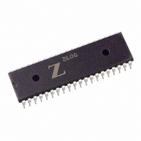
Z85C3010PSG Zilog, Z85C3010PSG Datasheet - Page 298

Z85C3010PSG
Manufacturer Part Number
Z85C3010PSG
Description
IC 10MHZ Z8500 CMOS SCC 40-DIP
Manufacturer
Zilog
Series
SCCr
Specifications of Z85C3010PSG
Processor Type
Z80
Features
Error Detection and Multiprotocol Support
Speed
10MHz
Voltage
5V
Mounting Type
Through Hole
Package / Case
40-DIP (0.620", 15.75mm)
Cpu Speed
8MHz
Digital Ic Case Style
DIP
No. Of Pins
40
Supply Voltage Range
5V
Operating Temperature Range
0°C To +70°C
Svhc
No SVHC (18-Jun-2010)
Base Number
85
Rohs Compliant
Yes
Clock Frequency
10MHz
Lead Free Status / RoHS Status
Lead free / RoHS Compliant
Other names
269-3934
Z85C3010PSG
Z85C3010PSG
Available stocks
Company
Part Number
Manufacturer
Quantity
Price
Company:
Part Number:
Z85C3010PSG
Manufacturer:
Zilog
Quantity:
135
Company:
Part Number:
Z85C3010PSG
Manufacturer:
Zilog
Quantity:
326
- Current page: 298 of 317
- Download datasheet (4Mb)
UM010901-0601
BUS DATA TRANSFERS
All data transfers to and from the ISCC™ are done in bytes
regardless of whether data occupies the lower or upper
byte of the 16-bit bus. Bus transfers as a slave peripheral
are done differently from bus transfers when the ISCC is
the bus master during DMA transactions. The ISCC is
fundamentally an 8-bit peripheral but supports 16-bit
buses in the DMA mode. Slave peripheral and DMA
transactions appear in the next sections.
Data Bus Transfers as a Slave Peripheral
When accessed as a peripheral device (when the ISCC is
not a bus master performing DMA transfers), only 8 bits
transfer. During ISCC register read, the byte data present
on the lower 8 bits of the bus is replicated on the upper 8
bits of the bus. Data is accepted by the ISCC only on the
lower 8 bits of the bus.
Write Register 0 (non-multiplexed bus mode)
D7
0
0
1
1
* With Point High Command
Figure 1. Write Register 0 Bit Functions
D6
0
1
0
1
D5 D4 D3 D2 D1 D0
0
0
0
0
1
1
1
1
Null Code
Reset Rx CRC Checker
Reset Tx CRC Generator
Reset Tx Underrun/EOM Latch
(Non-Multiplexed Bus Mode)
0
0
1
1
0
0
1
1
0
1
0
1
0
1
0
1
0
0
0
0
1
1
1
1
0
0
0
0
1
1
1
1
Null Code
Point High
Reset Ext/Status Interrupts
Send Abort (SDLC)
Enable Int on Next Rx Character
Reset Tx Int Pending
Error Reset
Reset Highest IUS
0
0
1
1
0
0
1
1
0
0
1
1
0
0
1
1
0
1
0
1
0
1
0
1
0
1
0
1
0
1
0
1
Register 0
Register 1
Register 2
Register 3
Register 4
Register 5
Register 6
Register 7
Register 8
Register 9
Register 10
Register 11
Register 12
Register 13
Register 14
Register 15
*
0
0
0
0
nnel Only
Null Code
Reset Rx CRC Checker
Reset Tx CRC Generator
Reset Tx Underrun/EOM Latch
5 D4 D3 D2 D1 D0
ster 0 (multiplexed bus mode)
ISCC
During DMA transfers, when the ISCC is bus master, only
byte data transfers occur. However, data transfers to or
from the ISCC on the upper 8 bits of the bus or on the lower
8 bits of the bus. Moreover, odd or even byte transfers
activate on the lower or upper 8 bits of the bus. This is
programmable and explained next.
During DMA transfers to memory from the ISCC, only byte
data transfers occur. Data appears on the lower 8 bits and
replicates on the upper 8 bits of the bus. Thus, the data is
written to an odd or even byte of the system memory by
address decoding and strobe generation.
During DMA transfers to the ISCC from memory, byte data
only transfers. Normally, data appears only on the lower 8
bits of the bus. However, the byte swapping feature
0
0
1
1
0
0
1
1
™
0
1
0
1
0
1
0
1
Figure 2. Write Register 0 Bit Functions
DMA Bus Transfers
Interfacing the ISCC™ to the 68000 and 8086
Null Code
Null Code
Reset Ext/Status Interrupts
Send Abort
Enable Int on Next Rx Character
Reset Tx Int Pending
Error Reset
Reset Highest IUS
0
0
1
1
(Multiplexed Bus Mode)
0
1
0
1
Null Code
Null Code
Select Shift Left Mode
Select Shift Right Mode
0
Application Note
*
6-3
Related parts for Z85C3010PSG
Image
Part Number
Description
Manufacturer
Datasheet
Request
R

Part Number:
Description:
Manufacturer:
Zilog, Inc.
Datasheet:

Part Number:
Description:
Cmos Scc Serial Communications Controller
Manufacturer:
ZiLOG Semiconductor
Datasheet:

Part Number:
Description:
Communication Controllers, ZILOG INTELLIGENT PERIPHERAL CONTROLLER (ZIP)
Manufacturer:
Zilog, Inc.
Datasheet:

Part Number:
Description:
KIT DEV FOR Z8 ENCORE 16K TO 64K
Manufacturer:
Zilog
Datasheet:

Part Number:
Description:
KIT DEV Z8 ENCORE XP 28-PIN
Manufacturer:
Zilog
Datasheet:

Part Number:
Description:
DEV KIT FOR Z8 ENCORE 8K/4K
Manufacturer:
Zilog
Datasheet:

Part Number:
Description:
KIT DEV Z8 ENCORE XP 28-PIN
Manufacturer:
Zilog
Datasheet:

Part Number:
Description:
DEV KIT FOR Z8 ENCORE 4K TO 8K
Manufacturer:
Zilog
Datasheet:

Part Number:
Description:
CMOS Z8 microcontroller. ROM 16 Kbytes, RAM 256 bytes, speed 16 MHz, 32 lines I/O, 3.0V to 5.5V
Manufacturer:
Zilog, Inc.
Datasheet:

Part Number:
Description:
Low-cost microcontroller. 512 bytes ROM, 61 bytes RAM, 8 MHz
Manufacturer:
Zilog, Inc.
Datasheet:

Part Number:
Description:
Z8 4K OTP Microcontroller
Manufacturer:
Zilog, Inc.
Datasheet:

Part Number:
Description:
CMOS SUPER8 ROMLESS MCU
Manufacturer:
Zilog, Inc.
Datasheet:

Part Number:
Description:
SL1866 CMOSZ8 OTP Microcontroller
Manufacturer:
Zilog, Inc.
Datasheet:


