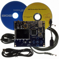
ATEVK1105 Atmel, ATEVK1105 Datasheet - Page 191

ATEVK1105
Manufacturer Part Number
ATEVK1105
Description
KIT EVAL FOR AT32UC3A0
Manufacturer
Atmel
Series
AVR®32r
Type
MCUr
Datasheets
1.ATAVRONE-PROBECBL.pdf
(16 pages)
2.ATEVK1104.pdf
(826 pages)
3.ATEVK1105.pdf
(28 pages)
Specifications of ATEVK1105
Contents
Evaluation Board, Software and Documentation
Processor To Be Evaluated
AT32UC3A0512
Processor Series
AVR
Data Bus Width
32 bit
Interface Type
USART, TWI, USB, SPI, Ethernet
Operating Supply Voltage
3.3 V
Silicon Manufacturer
Atmel
Core Architecture
AVR
Core Sub-architecture
AVR UC3
Silicon Core Number
AT32UC3A0512
Silicon Family Name
AVR
Kit Contents
Board CD Docs
Rohs Compliant
Yes
For Use With/related Products
AT32UC3A0
Lead Free Status / RoHS Status
Lead free / RoHS Compliant
- Current page: 191 of 826
- Download datasheet (20Mb)
23. Serial Peripheral Interface (SPI)
23.1
23.2
32058J–AVR32–04/11
Features
Description
Rev: 1.9.9.3
•
•
•
The Serial Peripheral Interface (SPI) circuit is a synchronous serial data link that provides com-
munication with external devices in Master or Slave Mode. It also enables communication
between processors if an external processor is connected to the system.
The Serial Peripheral Interface is essentially a shift register that serially transmits data bits to
other SPIs. During a data transfer, one SPI system acts as the “master”' which controls the data
flow, while the other devices act as “slaves'' which have data shifted into and out by the master.
Different CPUs can take turn being masters (Multiple Master Protocol opposite to Single Master
Protocol where one CPU is always the master while all of the others are always slaves) and one
master may simultaneously shift data into multiple slaves. However, only one slave may drive its
output to write data back to the master at any given time.
A slave device is selected when the master asserts its NSS signal. If multiple slave devices
exist, the master generates a separate slave select signal for each slave (NPCS).
The SPI system consists of two data lines and two control lines:
• Master Out Slave In (MOSI): This data line supplies the output data from the master shifted
• Master In Slave Out (MISO): This data line supplies the output data from a slave to the input of
• Serial Clock (SPCK): This control line is driven by the master and regulates the flow of the data
• Slave Select (NSS): This control line allows slaves to be turned on and off by hardware.
into the input(s) of the slave(s).
the master. There may be no more than one slave transmitting data during any particular
transfer.
bits. The master may transmit data at a variety of baud rates; the SPCK line cycles once for
each bit that is transmitted.
Supports Communication with Serial External Devices
Master or Slave Serial Peripheral Bus Interface
Connection to PDC Channel Capabilities Optimizes Data Transfers
– Four Chip Selects with External Decoder Support Allow Communication with Up to 15
– Serial Memories, such as DataFlash and 3-wire EEPROMs
– Serial Peripherals, such as ADCs, DACs, LCD Controllers, CAN Controllers and Sensors
– External Co-processors
– 8- to 16-bit Programmable Data Length Per Chip Select
– Programmable Phase and Polarity Per Chip Select
– Programmable Transfer Delays Between Consecutive Transfers and Between Clock and Data
– Programmable Delay Between Consecutive Transfers
– Selectable Mode Fault Detection
– One Channel for the Receiver, One Channel for the Transmitter
– Next Buffer Support
Peripherals
Per Chip Select
AT32UC3A
191
Related parts for ATEVK1105
Image
Part Number
Description
Manufacturer
Datasheet
Request
R

Part Number:
Description:
DEV KIT FOR AVR/AVR32
Manufacturer:
Atmel
Datasheet:

Part Number:
Description:
INTERVAL AND WIPE/WASH WIPER CONTROL IC WITH DELAY
Manufacturer:
ATMEL Corporation
Datasheet:

Part Number:
Description:
Low-Voltage Voice-Switched IC for Hands-Free Operation
Manufacturer:
ATMEL Corporation
Datasheet:

Part Number:
Description:
MONOLITHIC INTEGRATED FEATUREPHONE CIRCUIT
Manufacturer:
ATMEL Corporation
Datasheet:

Part Number:
Description:
AM-FM Receiver IC U4255BM-M
Manufacturer:
ATMEL Corporation
Datasheet:

Part Number:
Description:
Monolithic Integrated Feature Phone Circuit
Manufacturer:
ATMEL Corporation
Datasheet:

Part Number:
Description:
Multistandard Video-IF and Quasi Parallel Sound Processing
Manufacturer:
ATMEL Corporation
Datasheet:

Part Number:
Description:
High-performance EE PLD
Manufacturer:
ATMEL Corporation
Datasheet:

Part Number:
Description:
8-bit Flash Microcontroller
Manufacturer:
ATMEL Corporation
Datasheet:

Part Number:
Description:
2-Wire Serial EEPROM
Manufacturer:
ATMEL Corporation
Datasheet:


