ATEVK1105 Atmel, ATEVK1105 Datasheet - Page 400
ATEVK1105
Manufacturer Part Number
ATEVK1105
Description
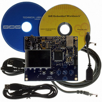
KIT EVAL FOR AT32UC3A0
Manufacturer
Atmel
Series
AVR®32r
Type
MCUr
Datasheets
1.ATAVRONE-PROBECBL.pdf
(16 pages)
2.ATEVK1104.pdf
(826 pages)
3.ATEVK1105.pdf
(28 pages)
Specifications of ATEVK1105
Contents
Evaluation Board, Software and Documentation
Processor To Be Evaluated
AT32UC3A0512
Processor Series
AVR
Data Bus Width
32 bit
Interface Type
USART, TWI, USB, SPI, Ethernet
Operating Supply Voltage
3.3 V
Silicon Manufacturer
Atmel
Core Architecture
AVR
Core Sub-architecture
AVR UC3
Silicon Core Number
AT32UC3A0512
Silicon Family Name
AVR
Kit Contents
Board CD Docs
Rohs Compliant
Yes
For Use With/related Products
AT32UC3A0
Lead Free Status / RoHS Status
Lead free / RoHS Compliant


Figure 27-34. Recommended Procedure to Switch from Slow Clock Mode to Normal Mode or from Normal Mode to Slow
27.6.9
27.6.9.1
32058J–AVR32–04/11
Internal signal from PM
Slow Clock Mode
NBS0, NBS1,
Asynchronous Page Mode
A0, A1
CLK_SMC
Protocol and Timings in Page Mode
A[25:2]
Clock Mode
NWE
NCS
The SMC supports asynchronous burst reads in page mode, providing that the page mode is
enabled in the MODE register (PMEN field). The page size must be configured in the MODE
register (PS field) to 4, 8, 16 or 32 bytes.
The page defines a set of consecutive bytes into memory. A 4-byte page (resp. 8-, 16-, 32-byte
page) is always aligned to 4-byte boundaries (resp. 8-, 16-, 32-byte boundaries) of memory. The
MSB of data address defines the address of the page in memory, the LSB of address define the
address of the data in the page as detailed in
With page mode memory devices, the first access to one page (t
quent accesses to the page (t
enables the user to define different read timings for the first access within one page, and next
accesses within the page.
Table 27-5.
Notes:
Figure 27-35
SLOW CLOCK MODE WRITE
Page Size
4 bytes
8 bytes
16 bytes
32 bytes
1
1. A denotes the address bus of the memory device
2. For 16-bit devices, the bit 0 of address is ignored. For 32-bit devices, bits [1:0] are ignored.
1
shows the NRD and NCS timings in page mode access.
Page Address and Data Address within a Page
Page Address
A[25:2]
A[25:3]
A[25:4]
A[25:5]
1
sa
) as shown in
(1)
IDLE STATE
Table
Figure
Reload Configuration
27-5.
Data Address in the Page
A[1:0]
A[2:0]
A[3:0]
A[4:0]
Wait State
27-35. When in page mode, the SMC
2
pa
NORMAL MODE WRITE
) takes longer than the subse-
3
AT32UC3A
(2)
2
400
Related parts for ATEVK1105
Image
Part Number
Description
Manufacturer
Datasheet
Request
R

Part Number:
Description:
DEV KIT FOR AVR/AVR32
Manufacturer:
Atmel
Datasheet:

Part Number:
Description:
INTERVAL AND WIPE/WASH WIPER CONTROL IC WITH DELAY
Manufacturer:
ATMEL Corporation
Datasheet:
Part Number:
Description:
Low-Voltage Voice-Switched IC for Hands-Free Operation
Manufacturer:
ATMEL Corporation
Datasheet:
Part Number:
Description:
MONOLITHIC INTEGRATED FEATUREPHONE CIRCUIT
Manufacturer:
ATMEL Corporation
Datasheet:
Part Number:
Description:
AM-FM Receiver IC U4255BM-M
Manufacturer:
ATMEL Corporation
Datasheet:
Part Number:
Description:
Monolithic Integrated Feature Phone Circuit
Manufacturer:
ATMEL Corporation
Datasheet:
Part Number:
Description:
Multistandard Video-IF and Quasi Parallel Sound Processing
Manufacturer:
ATMEL Corporation
Datasheet:
Part Number:
Description:
High-performance EE PLD
Manufacturer:
ATMEL Corporation
Datasheet:
Part Number:
Description:
8-bit Flash Microcontroller
Manufacturer:
ATMEL Corporation
Datasheet:
Part Number:
Description:
2-Wire Serial EEPROM
Manufacturer:
ATMEL Corporation
Datasheet: