ATEVK1105 Atmel, ATEVK1105 Datasheet - Page 204
ATEVK1105
Manufacturer Part Number
ATEVK1105
Description
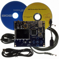
KIT EVAL FOR AT32UC3A0
Manufacturer
Atmel
Series
AVR®32r
Type
MCUr
Datasheets
1.ATAVRONE-PROBECBL.pdf
(16 pages)
2.ATEVK1104.pdf
(826 pages)
3.ATEVK1105.pdf
(28 pages)
Specifications of ATEVK1105
Contents
Evaluation Board, Software and Documentation
Processor To Be Evaluated
AT32UC3A0512
Processor Series
AVR
Data Bus Width
32 bit
Interface Type
USART, TWI, USB, SPI, Ethernet
Operating Supply Voltage
3.3 V
Silicon Manufacturer
Atmel
Core Architecture
AVR
Core Sub-architecture
AVR UC3
Silicon Core Number
AT32UC3A0512
Silicon Family Name
AVR
Kit Contents
Board CD Docs
Rohs Compliant
Yes
For Use With/related Products
AT32UC3A0
Lead Free Status / RoHS Status
Lead free / RoHS Compliant


23.7.3.8
23.7.4
32058J-AVR32-04/11
SPI Slave Mode
Mode Fault Detection
A mode fault is detected when the SPI is programmed in Master Mode and a low level is driven
by an external master on the NPCS0/NSS signal. NPCS0, MOSI, MISO and SPCK must be con-
figured in open-drain through the PIO controller, so that external pull up resistors are needed to
guarantee high level.
When a mode fault is detected, the MODF bit in the SR is set until the SR is read and the SPI is
automatically disabled until re-enabled by writing the SPIEN bit in the CR (Control Register) at 1.
By default, the Mode Fault detection circuitry is enabled. The user can disable Mode Fault
detection by setting the MODFDIS bit in the SPI Mode Register (MR).
When operating in Slave Mode, the SPI processes data bits on the clock provided on the SPI
clock pin (SPCK).
The SPI waits for NSS to go active before receiving the serial clock from an external master.
When NSS falls, the clock is validated on the serializer, which processes the number of bits
defined by the BITS field of the Chip Select Register 0 (CSR0). These bits are processed follow-
ing a phase and a polarity defined respectively by the NCPHA and CPOL bits of the CSR0. Note
that BITS, CPOL and NCPHA of the other Chip Select Registers have no effect when the SPI is
programmed in Slave Mode.
The bits are shifted out on the MISO line and sampled on the MOSI line.
When all the bits are processed, the received data is transferred in the Receive Data Register
and the RDRF bit rises. If RDRF is already high when the data is transferred, the Overrun bit
rises and the data transfer to RDR is aborted.
When a transfer starts, the data shifted out is the data present in the Shift Register. If no data
has been written in the Transmit Data Register (TDR), the last data received is transferred. If no
data has been received since the last reset, all bits are transmitted low, as the Shift Register
resets at 0.
When a first data is written in TDR, it is transferred immediately in the Shift Register and the
TDRE bit rises. If new data is written, it remains in TDR until a transfer occurs, i.e. NSS falls and
there is a valid clock on the SPCK pin. When the transfer occurs, the last data written in TDR is
transferred in the Shift Register and the TDRE bit rises. This enables frequent updates of critical
variables with single transfers.
Then, a new data is loaded in the Shift Register from the Transmit Data Register. In case no
character is ready to be transmitted, i.e. no character has been written in TDR since the last load
from TDR to the Shift Register, the Shift Register is not modified and the last received character
is retransmitted.
Figure 23-9
shows a block diagram of the SPI when operating in Slave Mode.
AT32UC3A
204
Related parts for ATEVK1105
Image
Part Number
Description
Manufacturer
Datasheet
Request
R

Part Number:
Description:
DEV KIT FOR AVR/AVR32
Manufacturer:
Atmel
Datasheet:

Part Number:
Description:
INTERVAL AND WIPE/WASH WIPER CONTROL IC WITH DELAY
Manufacturer:
ATMEL Corporation
Datasheet:
Part Number:
Description:
Low-Voltage Voice-Switched IC for Hands-Free Operation
Manufacturer:
ATMEL Corporation
Datasheet:
Part Number:
Description:
MONOLITHIC INTEGRATED FEATUREPHONE CIRCUIT
Manufacturer:
ATMEL Corporation
Datasheet:
Part Number:
Description:
AM-FM Receiver IC U4255BM-M
Manufacturer:
ATMEL Corporation
Datasheet:
Part Number:
Description:
Monolithic Integrated Feature Phone Circuit
Manufacturer:
ATMEL Corporation
Datasheet:
Part Number:
Description:
Multistandard Video-IF and Quasi Parallel Sound Processing
Manufacturer:
ATMEL Corporation
Datasheet:
Part Number:
Description:
High-performance EE PLD
Manufacturer:
ATMEL Corporation
Datasheet:
Part Number:
Description:
8-bit Flash Microcontroller
Manufacturer:
ATMEL Corporation
Datasheet:
Part Number:
Description:
2-Wire Serial EEPROM
Manufacturer:
ATMEL Corporation
Datasheet: