ATEVK1105 Atmel, ATEVK1105 Datasheet - Page 814
ATEVK1105
Manufacturer Part Number
ATEVK1105
Description
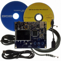
KIT EVAL FOR AT32UC3A0
Manufacturer
Atmel
Series
AVR®32r
Type
MCUr
Datasheets
1.ATAVRONE-PROBECBL.pdf
(16 pages)
2.ATEVK1104.pdf
(826 pages)
3.ATEVK1105.pdf
(28 pages)
Specifications of ATEVK1105
Contents
Evaluation Board, Software and Documentation
Processor To Be Evaluated
AT32UC3A0512
Processor Series
AVR
Data Bus Width
32 bit
Interface Type
USART, TWI, USB, SPI, Ethernet
Operating Supply Voltage
3.3 V
Silicon Manufacturer
Atmel
Core Architecture
AVR
Core Sub-architecture
AVR UC3
Silicon Core Number
AT32UC3A0512
Silicon Family Name
AVR
Kit Contents
Board CD Docs
Rohs Compliant
Yes
For Use With/related Products
AT32UC3A0
Lead Free Status / RoHS Status
Lead free / RoHS Compliant


41.5.11
41.5.12
41.5.13
32058J–AVR32–04/11
ABDAC
FLASHC
RTC
1. Audio Bitstream DAC is not functional.
1. The address of Flash General Purpose Fuse Register Low (FGPFRLO) is 0xFFFE140C
2. The command Quick Page Read User Page(QPRUP) is not functional.
3. PAGEN Semantic Field for Program GP Fuse Byte is WriteData[7:0], ByteAddress[1:0]
4. On AT32UC3A0512 and AT32UC3A1512, corrupted read in flash after FLASHC WP,
1. Writes to control (CTRL), top (TOP) and value (VAL) in the RTC are discarded if the
If the ADC sleep mode is activated when the ADC is idle the ADC will not enter sleep mode
before after the next AD conversion.
Fix/Workaround
Activate the sleep mode in the mode register and then perform an AD conversion.
Fix/Workaround
Do not use the ABDAC on revE.
on revE instead of 0xFFFE1410.
Fix/Workaround
None.
Fix/Workaround
None.
on revision E instead of WriteData[7:0], ByteAddress[2:0].
Fix/Workaround
None.
EP, EA, WUP, EUP commands may happen
- After a FLASHC Write Page (WP) or Erase Page (EP) command applied to a page in a
given half of the flash (first or last 256 kB of flash), reading (data read or code fetch) the
other half of the flash may fail. This may lead to an exception or to other errors derived from
this corrupted read access.
- After a FLASHC Erase All (EA) command, reading (data read or code fetch) the flash may
fail. This may lead to an exception or to other errors derived from this corrupted read access.
- After a FLASHC Write User Page (WUP) or Erase User Page (EUP) command, reading
(data read or code fetch) the second half (last 256 kB) of the flash may fail. This may lead to
an exception or to other errors derived from this corrupted read access.
Fix/Workaround
Flashc WP, EP, EA, WUP, EUP commands: these commands must be issued from RAM or
through the EBI. After these commands, read twice one flash page initialized to 00h in each
half part of the flash.
RTC peripheral bus clock (PBA) is divided by a factor of four or more relative to the
HSB clock.
Fix/Workaround
Do not write to the RTC registers using the peripheral bus clock (PBA) divided by a factor of
four or more relative to the HSB clock.
814
Related parts for ATEVK1105
Image
Part Number
Description
Manufacturer
Datasheet
Request
R

Part Number:
Description:
DEV KIT FOR AVR/AVR32
Manufacturer:
Atmel
Datasheet:

Part Number:
Description:
INTERVAL AND WIPE/WASH WIPER CONTROL IC WITH DELAY
Manufacturer:
ATMEL Corporation
Datasheet:
Part Number:
Description:
Low-Voltage Voice-Switched IC for Hands-Free Operation
Manufacturer:
ATMEL Corporation
Datasheet:
Part Number:
Description:
MONOLITHIC INTEGRATED FEATUREPHONE CIRCUIT
Manufacturer:
ATMEL Corporation
Datasheet:
Part Number:
Description:
AM-FM Receiver IC U4255BM-M
Manufacturer:
ATMEL Corporation
Datasheet:
Part Number:
Description:
Monolithic Integrated Feature Phone Circuit
Manufacturer:
ATMEL Corporation
Datasheet:
Part Number:
Description:
Multistandard Video-IF and Quasi Parallel Sound Processing
Manufacturer:
ATMEL Corporation
Datasheet:
Part Number:
Description:
High-performance EE PLD
Manufacturer:
ATMEL Corporation
Datasheet:
Part Number:
Description:
8-bit Flash Microcontroller
Manufacturer:
ATMEL Corporation
Datasheet:
Part Number:
Description:
2-Wire Serial EEPROM
Manufacturer:
ATMEL Corporation
Datasheet: