ATEVK1105 Atmel, ATEVK1105 Datasheet - Page 757
ATEVK1105
Manufacturer Part Number
ATEVK1105
Description
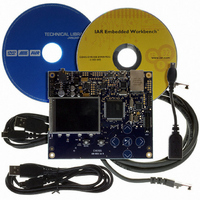
KIT EVAL FOR AT32UC3A0
Manufacturer
Atmel
Series
AVR®32r
Type
MCUr
Datasheets
1.ATAVRONE-PROBECBL.pdf
(16 pages)
2.ATEVK1104.pdf
(826 pages)
3.ATEVK1105.pdf
(28 pages)
Specifications of ATEVK1105
Contents
Evaluation Board, Software and Documentation
Processor To Be Evaluated
AT32UC3A0512
Processor Series
AVR
Data Bus Width
32 bit
Interface Type
USART, TWI, USB, SPI, Ethernet
Operating Supply Voltage
3.3 V
Silicon Manufacturer
Atmel
Core Architecture
AVR
Core Sub-architecture
AVR UC3
Silicon Core Number
AT32UC3A0512
Silicon Family Name
AVR
Kit Contents
Board CD Docs
Rohs Compliant
Yes
For Use With/related Products
AT32UC3A0
Lead Free Status / RoHS Status
Lead free / RoHS Compliant


36.9.8
36.9.9
36.9.10
32058J–AVR32–04/11
SYNC
AVR_RESET
CHIP_ERASE
This instruction allows external debuggers and testers to measure the ratio between the external
JTAG clock and the internal system clock. The SYNC data register is a 16-bit counter that
counts down to zero using the internal system clock. The busy bit stays high until the counter
reaches zero.
Starting in Run-Test/Idle, SYNC instruction is used in the following way:
The full 16-bit counter value must be provided when starting the synch operation, or the result
will be undefined. When reading status, shifting may be terminated once the required number of
bits have been acquired.
Table 36-12. SYNC_ACCESS details
This instruction allows a debugger or tester to directly control separate reset domains inside the
chip. The shift register contains one bit for each controllable reset domain. Setting a bit to one
resets that domain and holds it in reset. Setting a bit to zero releases the reset for that domain.
See the device specific documentation for the number of reset domains, and what these
domains are.
For any operation, all bits must be provided or the result will be undefined.
Table 36-13. AVR_RESET details
This instruction allows a programmer to completely erase all nonvolatile memories in a chip.
This will also clear any security bits that are set, so the device can be accessed normally. In
Instructions
IR input value
IR output value
DR Size
DR input value
DR output value
Instructions
IR input value
IR output value
DR Size
DR input value
DR output value
1. Select the DR Scan path.
2. Scan in an 16-bit counter value.
3. Go to Update-DR and re-enter Select-DR Scan.
4. Scan out the busy bit, and retry until the busy bit clears.
5. Calculate an approximation to the internal clock speed using the elapsed time and the
6. Return to Run-Test/Idle.
counter value.
Details
10111 (0x17)
peb01
16 bits
dddddddd dddddddd
xxxxxxxx xxxxxxeb
Details
01100 (0x0C)
p0001
Device specific.
Device specific.
Device specific.
AT32UC3A
757
Related parts for ATEVK1105
Image
Part Number
Description
Manufacturer
Datasheet
Request
R

Part Number:
Description:
DEV KIT FOR AVR/AVR32
Manufacturer:
Atmel
Datasheet:

Part Number:
Description:
INTERVAL AND WIPE/WASH WIPER CONTROL IC WITH DELAY
Manufacturer:
ATMEL Corporation
Datasheet:
Part Number:
Description:
Low-Voltage Voice-Switched IC for Hands-Free Operation
Manufacturer:
ATMEL Corporation
Datasheet:
Part Number:
Description:
MONOLITHIC INTEGRATED FEATUREPHONE CIRCUIT
Manufacturer:
ATMEL Corporation
Datasheet:
Part Number:
Description:
AM-FM Receiver IC U4255BM-M
Manufacturer:
ATMEL Corporation
Datasheet:
Part Number:
Description:
Monolithic Integrated Feature Phone Circuit
Manufacturer:
ATMEL Corporation
Datasheet:
Part Number:
Description:
Multistandard Video-IF and Quasi Parallel Sound Processing
Manufacturer:
ATMEL Corporation
Datasheet:
Part Number:
Description:
High-performance EE PLD
Manufacturer:
ATMEL Corporation
Datasheet:
Part Number:
Description:
8-bit Flash Microcontroller
Manufacturer:
ATMEL Corporation
Datasheet:
Part Number:
Description:
2-Wire Serial EEPROM
Manufacturer:
ATMEL Corporation
Datasheet: