ATEVK1105 Atmel, ATEVK1105 Datasheet - Page 198
ATEVK1105
Manufacturer Part Number
ATEVK1105
Description
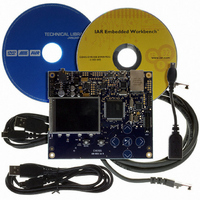
KIT EVAL FOR AT32UC3A0
Manufacturer
Atmel
Series
AVR®32r
Type
MCUr
Datasheets
1.ATAVRONE-PROBECBL.pdf
(16 pages)
2.ATEVK1104.pdf
(826 pages)
3.ATEVK1105.pdf
(28 pages)
Specifications of ATEVK1105
Contents
Evaluation Board, Software and Documentation
Processor To Be Evaluated
AT32UC3A0512
Processor Series
AVR
Data Bus Width
32 bit
Interface Type
USART, TWI, USB, SPI, Ethernet
Operating Supply Voltage
3.3 V
Silicon Manufacturer
Atmel
Core Architecture
AVR
Core Sub-architecture
AVR UC3
Silicon Core Number
AT32UC3A0512
Silicon Family Name
AVR
Kit Contents
Board CD Docs
Rohs Compliant
Yes
For Use With/related Products
AT32UC3A0
Lead Free Status / RoHS Status
Lead free / RoHS Compliant


23.7.3
32058J–AVR32–04/11
Master Mode Operations
When configured in Master Mode, the SPI uses the internal programmable baud rate generator
as clock source. It fully controls the data transfers to and from the slave(s) connected to the SPI
bus. The SPI drives the chip select line to the slave and the serial clock signal (SPCK).
The SPI features two holding registers, the Transmit Data Register and the Receive Data Regis-
ter, and a single Shift Register. The holding registers maintain the data flow at a constant rate.
After enabling the SPI, a data transfer begins when the processor writes to the TDR (Transmit
Data Register). The written data is immediately transferred in the Shift Register and transfer on
the SPI bus starts. While the data in the Shift Register is shifted on the MOSI line, the MISO line
is sampled and shifted in the Shift Register. Transmission cannot occur without reception.
Before writing the TDR, the PCS field must be set in order to select a slave.
If new data is written in TDR during the transfer, it stays in it until the current transfer is com-
pleted. Then, the received data is transferred from the Shift Register to RDR, the data in TDR is
loaded in the Shift Register and a new transfer starts.
The transfer of a data written in TDR in the Shift Register is indicated by the TDRE bit (Transmit
Data Register Empty) in the Status Register (SR). When new data is written in TDR, this bit is
cleared. The TDRE bit is used to trigger the Transmit PDC channel.
The end of transfer is indicated by the TXEMPTY flag in the SR register. If a transfer delay (DLY-
BCT) is greater than 0 for the last transfer, TXEMPTY is set after the completion of said delay.
The master clock (MCK) can be switched off at this time.
The transfer of received data from the Shift Register in RDR is indicated by the RDRF bit
(Receive Data Register Full) in the Status Register (SR). When the received data is read, the
RDRF bit is cleared.
If the RDR (Receive Data Register) has not been read before new data is received, the Overrun
Error bit (OVRES) in SR is set. When this bit is set the SPI will continue to update RDR when
data is received, overwriting the previously received data. The user has to read the status regis-
ter to clear the OVRES bit.
Figure 23-5 on page 199
ure 23-6 on page 200
shows a flow chart describing how transfers are handled.
shows a block diagram of the SPI when operating in Master Mode.
AT32UC3A
Fig-
198
Related parts for ATEVK1105
Image
Part Number
Description
Manufacturer
Datasheet
Request
R

Part Number:
Description:
DEV KIT FOR AVR/AVR32
Manufacturer:
Atmel
Datasheet:

Part Number:
Description:
INTERVAL AND WIPE/WASH WIPER CONTROL IC WITH DELAY
Manufacturer:
ATMEL Corporation
Datasheet:
Part Number:
Description:
Low-Voltage Voice-Switched IC for Hands-Free Operation
Manufacturer:
ATMEL Corporation
Datasheet:
Part Number:
Description:
MONOLITHIC INTEGRATED FEATUREPHONE CIRCUIT
Manufacturer:
ATMEL Corporation
Datasheet:
Part Number:
Description:
AM-FM Receiver IC U4255BM-M
Manufacturer:
ATMEL Corporation
Datasheet:
Part Number:
Description:
Monolithic Integrated Feature Phone Circuit
Manufacturer:
ATMEL Corporation
Datasheet:
Part Number:
Description:
Multistandard Video-IF and Quasi Parallel Sound Processing
Manufacturer:
ATMEL Corporation
Datasheet:
Part Number:
Description:
High-performance EE PLD
Manufacturer:
ATMEL Corporation
Datasheet:
Part Number:
Description:
8-bit Flash Microcontroller
Manufacturer:
ATMEL Corporation
Datasheet:
Part Number:
Description:
2-Wire Serial EEPROM
Manufacturer:
ATMEL Corporation
Datasheet: