MCHC908MR8VFAE Freescale Semiconductor, MCHC908MR8VFAE Datasheet - Page 120
MCHC908MR8VFAE
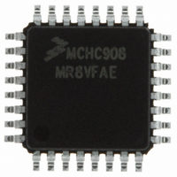
Manufacturer Part Number
MCHC908MR8VFAE
Description
IC MCU 8K FLASH 8MHZ PWM 32-LQFP
Manufacturer
Freescale Semiconductor
Series
HC08r
Datasheet
1.MCHC908MR8VFAE.pdf
(372 pages)
Specifications of MCHC908MR8VFAE
Core Processor
HC08
Core Size
8-Bit
Speed
8MHz
Connectivity
SCI
Peripherals
LVD, POR, PWM
Number Of I /o
16
Program Memory Size
8KB (8K x 8)
Program Memory Type
FLASH
Ram Size
256 x 8
Voltage - Supply (vcc/vdd)
4.5 V ~ 5.5 V
Data Converters
A/D 7x10b
Oscillator Type
Internal
Operating Temperature
-40°C ~ 105°C
Package / Case
32-LQFP
Processor Series
HC08MR
Core
HC08
Data Bus Width
8 bit
Data Ram Size
512 B
Interface Type
SCI, SPI
Maximum Clock Frequency
8 MHz
Number Of Programmable I/os
33
Number Of Timers
4
Maximum Operating Temperature
+ 105 C
Mounting Style
SMD/SMT
Development Tools By Supplier
FSICEBASE, M68CBL05CE
Minimum Operating Temperature
- 40 C
On-chip Adc
8 bit, 8 Channel
Lead Free Status / RoHS Status
Lead free / RoHS Compliant
Eeprom Size
-
Lead Free Status / Rohs Status
Details
Available stocks
Company
Part Number
Manufacturer
Quantity
Price
Company:

Part Number:
MCHC908MR8VFAE
Manufacturer:
Freescale
Quantity:
8 393
Company:
Part Number:
MCHC908MR8VFAE
Manufacturer:
Freescale Semiconductor
Quantity:
10 000


Clock Generator Module (CGM)
8.4.2.4 Programming the PLL
Technical Data
120
CAUTION:
NOTE:
This procedure shows how to program the PLL.
The round function in the following equations means that the real
number should be rounded to the nearest integer number.
Exceeding the recommended maximum bus frequency or VCO
frequency can crash the MCU.
1. Choose the desired bus frequency, f
2. Calculate the desired VCO frequency (four times the desired bus
3. Choose a practical PLL reference frequency, f
4. Select a VCO frequency multiplier, N.
5. Calculate and verify the adequacy of the VCO and bus
6. Select a VCO linear range multiplier, L.
7. Calculate and verify the adequacy of the VCO programmed
8. Verify the choice of N and L by comparing f
9. Program the PLL registers accordingly:
frequency).
frequencies f
where f
center-of-range frequency, f
f
application’s tolerance of f
possible to f
a. In the upper four bits of the PLL programming register (PPG),
b. In the lower four bits of the PLL programming register (PPG),
VCLKDES
program the binary equivalent of N.
program the binary equivalent of L.
Clock Generator Module (CGM)
NOM
. For proper operation, f
VCLK
= 4.9152 MHz
VCLK
f
.
VCLKDES
and f
f
f
VCLK
BUS
f
VRS
BUS
VCLKDES
=
= (L) f
.
=
=
VRS
(
N
f
4
VCLK
×
×
.
f
f
NOM
VCLK
RCLK
BUSDES
, and f
) 4 ⁄
BUSDES
must be within the
VRS
MC68HC908MR8 — Rev 4.1
VCLK
.
Freescale Semiconductor
must be as close as
RCLK
to f
.
VRS
and
Related parts for MCHC908MR8VFAE
Image
Part Number
Description
Manufacturer
Datasheet
Request
R

Part Number:
Description:
Manufacturer:
Freescale Semiconductor, Inc
Datasheet:
Part Number:
Description:
Manufacturer:
Freescale Semiconductor, Inc
Datasheet:
Part Number:
Description:
Manufacturer:
Freescale Semiconductor, Inc
Datasheet:
Part Number:
Description:
Manufacturer:
Freescale Semiconductor, Inc
Datasheet:
Part Number:
Description:
Manufacturer:
Freescale Semiconductor, Inc
Datasheet:
Part Number:
Description:
Manufacturer:
Freescale Semiconductor, Inc
Datasheet:
Part Number:
Description:
Manufacturer:
Freescale Semiconductor, Inc
Datasheet:
Part Number:
Description:
Manufacturer:
Freescale Semiconductor, Inc
Datasheet:
Part Number:
Description:
Manufacturer:
Freescale Semiconductor, Inc
Datasheet:
Part Number:
Description:
Manufacturer:
Freescale Semiconductor, Inc
Datasheet:
Part Number:
Description:
Manufacturer:
Freescale Semiconductor, Inc
Datasheet:
Part Number:
Description:
Manufacturer:
Freescale Semiconductor, Inc
Datasheet:
Part Number:
Description:
Manufacturer:
Freescale Semiconductor, Inc
Datasheet:
Part Number:
Description:
Manufacturer:
Freescale Semiconductor, Inc
Datasheet:
Part Number:
Description:
Manufacturer:
Freescale Semiconductor, Inc
Datasheet: