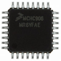
MCHC908MR8VFAE Freescale Semiconductor, MCHC908MR8VFAE Datasheet - Page 286

MCHC908MR8VFAE
Manufacturer Part Number
MCHC908MR8VFAE
Description
IC MCU 8K FLASH 8MHZ PWM 32-LQFP
Manufacturer
Freescale Semiconductor
Series
HC08r
Datasheet
1.MCHC908MR8VFAE.pdf
(372 pages)
Specifications of MCHC908MR8VFAE
Core Processor
HC08
Core Size
8-Bit
Speed
8MHz
Connectivity
SCI
Peripherals
LVD, POR, PWM
Number Of I /o
16
Program Memory Size
8KB (8K x 8)
Program Memory Type
FLASH
Ram Size
256 x 8
Voltage - Supply (vcc/vdd)
4.5 V ~ 5.5 V
Data Converters
A/D 7x10b
Oscillator Type
Internal
Operating Temperature
-40°C ~ 105°C
Package / Case
32-LQFP
Processor Series
HC08MR
Core
HC08
Data Bus Width
8 bit
Data Ram Size
512 B
Interface Type
SCI, SPI
Maximum Clock Frequency
8 MHz
Number Of Programmable I/os
33
Number Of Timers
4
Maximum Operating Temperature
+ 105 C
Mounting Style
SMD/SMT
Development Tools By Supplier
FSICEBASE, M68CBL05CE
Minimum Operating Temperature
- 40 C
On-chip Adc
8 bit, 8 Channel
Lead Free Status / RoHS Status
Lead free / RoHS Compliant
Eeprom Size
-
Lead Free Status / Rohs Status
Details
Available stocks
Company
Part Number
Manufacturer
Quantity
Price
Company:
Part Number:
MCHC908MR8VFAE
Manufacturer:
Freescale
Quantity:
8 393
Company:
Part Number:
MCHC908MR8VFAE
Manufacturer:
Freescale Semiconductor
Quantity:
10 000
- Current page: 286 of 372
- Download datasheet (4Mb)
Input/Output (I/O) Ports
14.5 Port C
Technical Data
286
When bit DDRBx is a logic 1, reading address $0001 reads the PTBx
data latch. When bit DDRBx is a logic 0, reading address $0001 reads
the voltage level on the pin. The data latch can always be written,
regardless of the state of its data direction bit.
the operation of the port B pins.
Port C is a 2-bit special-purpose I/O port sharing its pins with the pulse
width modulator for motor control module (PMC) FAULT input pins.
These two pins mirror the state of FAULT1 and FAULT4 pins. Level
changes on these input pins will be interpreted as fault conditions.
The port C data register contains a data latch for each of the two port
pins.
DDRB
1. X = don’t care
2. Hi-Z = high impedance
3. Writing affects data register, but does not affect input.
Bit
0
1
READ DDRB ($0005)
WRITE DDRB ($0005)
WRITE PTB ($0001)
READ PTB ($0001)
PTB
X
Bit
X
Input/Output (I/O) Ports
(1)
Table 14-2. Port B Pin Functions
Figure 14-7. Port B I/O Circuit
RESET
I/O Pin Mode
Input, Hi-Z
Output
(2)
DDRBx
PTBx
Read/Write
DDRB[6:0]
DDRB[6:0]
Accesses
to DDRB
Table 14-2
MC68HC908MR8 — Rev 4.1
Freescale Semiconductor
PTB[6:0]
Read
Accesses to PTB
Pin
summarizes
PTB[6:0]
PTB[6:0]
Write
PTBx
(3)
Related parts for MCHC908MR8VFAE
Image
Part Number
Description
Manufacturer
Datasheet
Request
R
Part Number:
Description:
Manufacturer:
Freescale Semiconductor, Inc
Datasheet:
Part Number:
Description:
Manufacturer:
Freescale Semiconductor, Inc
Datasheet:
Part Number:
Description:
Manufacturer:
Freescale Semiconductor, Inc
Datasheet:
Part Number:
Description:
Manufacturer:
Freescale Semiconductor, Inc
Datasheet:
Part Number:
Description:
Manufacturer:
Freescale Semiconductor, Inc
Datasheet:
Part Number:
Description:
Manufacturer:
Freescale Semiconductor, Inc
Datasheet:
Part Number:
Description:
Manufacturer:
Freescale Semiconductor, Inc
Datasheet:
Part Number:
Description:
Manufacturer:
Freescale Semiconductor, Inc
Datasheet:
Part Number:
Description:
Manufacturer:
Freescale Semiconductor, Inc
Datasheet:
Part Number:
Description:
Manufacturer:
Freescale Semiconductor, Inc
Datasheet:
Part Number:
Description:
Manufacturer:
Freescale Semiconductor, Inc
Datasheet:
Part Number:
Description:
Manufacturer:
Freescale Semiconductor, Inc
Datasheet:
Part Number:
Description:
Manufacturer:
Freescale Semiconductor, Inc
Datasheet:
Part Number:
Description:
Manufacturer:
Freescale Semiconductor, Inc
Datasheet:
Part Number:
Description:
Manufacturer:
Freescale Semiconductor, Inc
Datasheet:


