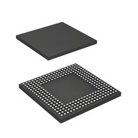
HD6417720BP133BV Renesas Electronics America, HD6417720BP133BV Datasheet - Page 462

HD6417720BP133BV
Manufacturer Part Number
HD6417720BP133BV
Description
SH3-DSP, WITH USB AND LCDC, PB-F
Manufacturer
Renesas Electronics America
Series
SuperH® SH7700r
Datasheet
1.R8A77210C133BAV.pdf
(1478 pages)
Specifications of HD6417720BP133BV
Core Processor
SH-3 DSP
Core Size
32-Bit
Speed
133MHz
Connectivity
FIFO, I²C, IrDA, MMC, SCI, SD, SIO, SIM, USB
Peripherals
DMA, LCD, POR, WDT
Number Of I /o
117
Program Memory Type
ROMless
Ram Size
16K x 8
Voltage - Supply (vcc/vdd)
1.4 V ~ 1.6 V
Data Converters
A/D 4x10b; D/A 2x8b
Oscillator Type
Internal
Operating Temperature
-20°C ~ 75°C
Package / Case
256-BGA
Lead Free Status / RoHS Status
Lead free / RoHS Compliant
Eeprom Size
-
Program Memory Size
-
- Current page: 462 of 1478
- Download datasheet (10Mb)
Section 9 Bus State Controller (BSC)
1. 16-byte transfer because of a cache miss
2. During copyback operation for the cache
3. Between the read and write cycles of a TAS instruction
4. Multiple bus cycles generated when the data bus width is smaller than the access size (for
5. 16-byte transfer by the DMAC or USBH
6. Setting the BLOCK bit in CMNCR to 1
7. 16 to 128-byte transfer by LCDC
8. Transfer by USBH
Bits DPRTY[1:0] in CMNCR can select whether or not the bus request is received during DMAC
burst transfer.
This LSI has the bus mastership until a bus request is received from another device. Upon
acknowledging the assertion (low level) of the external bus request signal BREQ, the LSI releases
the bus at the completion of the current bus cycle and asserts the BACK signal. After the LSI
acknowledges the negation (high level) of the BREQ signal that indicates the slave has released
the bus, it negates the BACK signal and resumes the bus usage.
The SDRAM issues an all bank precharge command (PALL) when active banks exist and releases
the bus after completion of a PALL command.
The bus sequence is as follows. The address bus and data bus are placed in a high-impedance state
synchronized with the rising edge of CKIO. The bus mastership enable signal is asserted 0.5
cycles after the above timing, synchronized with the falling edge of CKIO. The bus control signals
(BS, CSn, RAS, CAS, DQMxx, WEn (BEn), RD, and RD/WR) are placed in the high-impedance
state at subsequent rising edges of CKIO. Bus request signals are sampled at the falling edge of
CKIO.
The sequence for reclaiming the bus mastership from a slave is described below. 1.5 cycles after
the negation of BREQ is detected at the falling edge of CKIO, the bus control signals are driven
high. The BACK is negated at the next falling edge of the clock. The fastest timing at which actual
bus cycles can be resumed after bus control signal assertion is at the rising edge of the CKIO
where address and data signals are driven. Figure 9.45 shows the bus arbitration timing.
In an original slave device designed by the user, multiple bus accesses are generated continuously
to reduce the overhead caused by bus arbitration. In this case, to execute SDRAM refresh
correctly, the slave device must be designed to release the bus mastership within the refresh
interval time. To achieve this, the LSI instructs the REFOUT pin to request the bus mastership
Page 402 of 1414
example, between bus cycles when longword access is made to a memory with a data bus
width of 8 bits)
SH7720 Group, SH7721 Group
R01UH0083EJ0400 Rev. 4.00
Sep 21, 2010
Related parts for HD6417720BP133BV
Image
Part Number
Description
Manufacturer
Datasheet
Request
R

Part Number:
Description:
KIT STARTER FOR M16C/29
Manufacturer:
Renesas Electronics America
Datasheet:

Part Number:
Description:
KIT STARTER FOR R8C/2D
Manufacturer:
Renesas Electronics America
Datasheet:

Part Number:
Description:
R0K33062P STARTER KIT
Manufacturer:
Renesas Electronics America
Datasheet:

Part Number:
Description:
KIT STARTER FOR R8C/23 E8A
Manufacturer:
Renesas Electronics America
Datasheet:

Part Number:
Description:
KIT STARTER FOR R8C/25
Manufacturer:
Renesas Electronics America
Datasheet:

Part Number:
Description:
KIT STARTER H8S2456 SHARPE DSPLY
Manufacturer:
Renesas Electronics America
Datasheet:

Part Number:
Description:
KIT STARTER FOR R8C38C
Manufacturer:
Renesas Electronics America
Datasheet:

Part Number:
Description:
KIT STARTER FOR R8C35C
Manufacturer:
Renesas Electronics America
Datasheet:

Part Number:
Description:
KIT STARTER FOR R8CL3AC+LCD APPS
Manufacturer:
Renesas Electronics America
Datasheet:

Part Number:
Description:
KIT STARTER FOR RX610
Manufacturer:
Renesas Electronics America
Datasheet:

Part Number:
Description:
KIT STARTER FOR R32C/118
Manufacturer:
Renesas Electronics America
Datasheet:

Part Number:
Description:
KIT DEV RSK-R8C/26-29
Manufacturer:
Renesas Electronics America
Datasheet:

Part Number:
Description:
KIT STARTER FOR SH7124
Manufacturer:
Renesas Electronics America
Datasheet:

Part Number:
Description:
KIT STARTER FOR H8SX/1622
Manufacturer:
Renesas Electronics America
Datasheet:

Part Number:
Description:
KIT DEV FOR SH7203
Manufacturer:
Renesas Electronics America
Datasheet:


