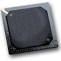
MPC564CZP40 Freescale Semiconductor, MPC564CZP40 Datasheet - Page 1050

MPC564CZP40
Manufacturer Part Number
MPC564CZP40
Description
IC MPU 32BIT W/CODE COMP 388PBGA
Manufacturer
Freescale Semiconductor
Series
MPC5xxr
Specifications of MPC564CZP40
Core Processor
PowerPC
Core Size
32-Bit
Speed
40MHz
Connectivity
CAN, EBI/EMI, SCI, SPI, UART/USART
Peripherals
POR, PWM, WDT
Number Of I /o
56
Program Memory Size
512KB (512K x 8)
Program Memory Type
FLASH
Ram Size
32K x 8
Voltage - Supply (vcc/vdd)
2.5 V ~ 2.7 V
Data Converters
A/D 32x10b
Oscillator Type
External
Operating Temperature
-40°C ~ 85°C
Package / Case
388-BGA
Processor Series
MPC5xx
Core
PowerPC
Data Bus Width
32 bit
Data Ram Size
32 KB
Interface Type
CAN, JTAG, QSPI, SCI, SPI, UART
Maximum Clock Frequency
40 MHz
Number Of Programmable I/os
56
Number Of Timers
2
Operating Supply Voltage
0 V to 5 V
Maximum Operating Temperature
+ 85 C
Mounting Style
SMD/SMT
Minimum Operating Temperature
- 40 C
On-chip Adc
2 (10 bit, 32 Channel)
For Use With
MPC564EVB - KIT EVAL FOR MPC561/562/563/564
Lead Free Status / RoHS Status
Contains lead / RoHS non-compliant
Eeprom Size
-
Lead Free Status / Rohs Status
No
Available stocks
Company
Part Number
Manufacturer
Quantity
Price
Company:
Part Number:
MPC564CZP40
Manufacturer:
Freescale Semiconductor
Quantity:
10 000
- Current page: 1050 of 1420
- Download datasheet (11Mb)
READI Module
24.14.3 Throughput
The tool can send a DSDI data message into device upon the receipt of a DSDO data message as soon as
the tool decodes the first two status bits of the DSDO data message just received and confirms valid data
from the RCPU.
An example throughput analysis is performed with the following assumptions:
The DSDI data message is 41 bits (six bits of TCODE and 35 bits of DSDI data.). It takes 41 clocks (41
bits / 1 MDI signals) to shift in the DSDI data message. It is estimated that READI will take approximately
10 clocks to decode the DSDI data message. After the message has been decoded, READI will take 35
clocks to serially shift in the 35 bits of DSDI data to the RCPU development port. Hence, it takes a total
of 86 clocks (41 + 10 + 35) to decode and shift in DSDI data from the tool to the RCPU development port.
At 28 MHz, it translates to 3079 ns (35.8 x 81) to decode and shift in DSDI data to RCPU development port
As DSDI bits are shifted into the RCPU development register, DSDO bits are shifted out from the same
RCPU development register (DPDR) and these are captured by READI.
It is estimated that READI will take approximately 10 clocks to encode the DSDO data. The DSDO
message is 41 bits (6 bits of TCODE and 35 bits of DSDO data). It will take 21 clocks (41 bits / 2 MDO
signals) for READI to transmit this message. Hence, it will take a total of 31 clocks (10 + 21) to encode
the DSDO data message and shift out the DSDO data message to the tool.
At 56 MHz, it will take 552 ns (17.8 x 31) to encode and shift out DSDO data to the tool.
Thus, it will take 3631 ns (3079 + 552) for one complete DSDI data and DSDO data messaging cycle.
24.14.4 Development Access Timing Diagrams
Figure 24-84
out-of-system reset through READI.
24-82
•
•
•
•
•
•
•
•
•
READI configuration of RCPU development access and debug mode is already entered through
READI
The module is configured for reduced port mode
MCKI running at 28 MHz
MCKO running at 56 MHz
56-MHz internal operation
READI auxiliary input and output signals are free (not in middle of transmission)
No delay from tool in responding — tool keeps up with READI port
Tool reads the complete DSDO data message before shifting in DSDI data message
10 clocks estimated to format and encode/decode DSDI data and DSDO data messages within
READI
shows the timing diagram of RCPU development access and entering debug mode
MPC561/MPC563 Reference Manual, Rev. 1.2
Freescale Semiconductor
Related parts for MPC564CZP40
Image
Part Number
Description
Manufacturer
Datasheet
Request
R

Part Number:
Description:
MPC5 1K0 5%
Manufacturer:
TE Connectivity
Datasheet:

Part Number:
Description:
MPC5 500R 5%
Manufacturer:
TE Connectivity
Datasheet:

Part Number:
Description:
MPC5 5K0 5%
Manufacturer:
Tyco Electronics
Datasheet:

Part Number:
Description:
MPC5 5R0 5%
Manufacturer:
Tyco Electronics
Datasheet:

Part Number:
Description:
MPC5 50K 5%
Manufacturer:
Tyco Electronics
Datasheet:

Part Number:
Description:
MPC5 1R0 5%
Manufacturer:
Tyco Electronics
Datasheet:
Part Number:
Description:
Manufacturer:
Freescale Semiconductor, Inc
Datasheet:
Part Number:
Description:
Manufacturer:
Freescale Semiconductor, Inc
Datasheet:
Part Number:
Description:
Manufacturer:
Freescale Semiconductor, Inc
Datasheet:
Part Number:
Description:
Manufacturer:
Freescale Semiconductor, Inc
Datasheet:
Part Number:
Description:
Manufacturer:
Freescale Semiconductor, Inc
Datasheet:


