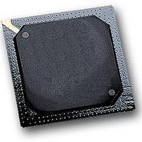
MPC564CZP40 Freescale Semiconductor, MPC564CZP40 Datasheet - Page 1321

MPC564CZP40
Manufacturer Part Number
MPC564CZP40
Description
IC MPU 32BIT W/CODE COMP 388PBGA
Manufacturer
Freescale Semiconductor
Series
MPC5xxr
Specifications of MPC564CZP40
Core Processor
PowerPC
Core Size
32-Bit
Speed
40MHz
Connectivity
CAN, EBI/EMI, SCI, SPI, UART/USART
Peripherals
POR, PWM, WDT
Number Of I /o
56
Program Memory Size
512KB (512K x 8)
Program Memory Type
FLASH
Ram Size
32K x 8
Voltage - Supply (vcc/vdd)
2.5 V ~ 2.7 V
Data Converters
A/D 32x10b
Oscillator Type
External
Operating Temperature
-40°C ~ 85°C
Package / Case
388-BGA
Processor Series
MPC5xx
Core
PowerPC
Data Bus Width
32 bit
Data Ram Size
32 KB
Interface Type
CAN, JTAG, QSPI, SCI, SPI, UART
Maximum Clock Frequency
40 MHz
Number Of Programmable I/os
56
Number Of Timers
2
Operating Supply Voltage
0 V to 5 V
Maximum Operating Temperature
+ 85 C
Mounting Style
SMD/SMT
Minimum Operating Temperature
- 40 C
On-chip Adc
2 (10 bit, 32 Channel)
For Use With
MPC564EVB - KIT EVAL FOR MPC561/562/563/564
Lead Free Status / RoHS Status
Contains lead / RoHS non-compliant
Eeprom Size
-
Lead Free Status / Rohs Status
No
Available stocks
Company
Part Number
Manufacturer
Quantity
Price
Company:
Part Number:
MPC564CZP40
Manufacturer:
Freescale Semiconductor
Quantity:
10 000
- Current page: 1321 of 1420
- Download datasheet (11Mb)
Figure G-4
G.9.2
A less stringent power-up sequence may be implemented if 2.6-V compliant pins and dual 2.6-V/5-V
compliant pins are NOT connected to the 5-V supply with a pull-up resistor or driven by 5-V logic during
power-up/down.
The option B power-up sequence (excluding V
Thus the V
no adverse affects to the device.
The requirement that V
dual 2.6-V/5-V compliant pins and 2.6-V pins. The diodes are forward biased when V
V
Figure G-5
power-up sequence if a keep-alive supply is required. The keep-alive supply should be powered-up at the
same time or before both the high voltage and low voltage supplies are powered-up.
Freescale Semiconductor
DDH
1. V
V
V
and will start to conduct current.
DDH
DDL
DDH
DDH
illustrates the power-up sequence if no keep-alive supply is required.
illustrates the power-down sequence if a keep-alive supply is required.
Power-Up/Down Option B
> V
supply group can be fully powered-up prior to power-up of the V
DDL
V
V
Figure G-4. Option A Power-Down Sequence With Keep-Alive Supply
DDH
DDH
- 0.5 V (V
DDH
≥ V
cannot lag V
DDL
cannot lag V
0.5-V Max
- 0.5 V (V
MPC561/MPC563 Reference Manual, Rev. 1.2
DDH
DDL
by more than 3.1 V.
DDH
cannot lag V
DDL
cannot lead V
by more than 0.5 V is due to ESD diodes in the pad logic for
DDKA
DDL
) is:
DDL
by more than 0.5 V)
3.1-V Max
by more than 0.5 V.)
Ramp down rates may
differ with load.
66-MHz Electrical Characteristics
V
Figure G-6
DDKA
DDL
supply group, with
DDL
is greater than
illustrates the
G-15
Related parts for MPC564CZP40
Image
Part Number
Description
Manufacturer
Datasheet
Request
R

Part Number:
Description:
MPC5 1K0 5%
Manufacturer:
TE Connectivity
Datasheet:

Part Number:
Description:
MPC5 500R 5%
Manufacturer:
TE Connectivity
Datasheet:

Part Number:
Description:
MPC5 5K0 5%
Manufacturer:
Tyco Electronics
Datasheet:

Part Number:
Description:
MPC5 5R0 5%
Manufacturer:
Tyco Electronics
Datasheet:

Part Number:
Description:
MPC5 50K 5%
Manufacturer:
Tyco Electronics
Datasheet:

Part Number:
Description:
MPC5 1R0 5%
Manufacturer:
Tyco Electronics
Datasheet:
Part Number:
Description:
Manufacturer:
Freescale Semiconductor, Inc
Datasheet:
Part Number:
Description:
Manufacturer:
Freescale Semiconductor, Inc
Datasheet:
Part Number:
Description:
Manufacturer:
Freescale Semiconductor, Inc
Datasheet:
Part Number:
Description:
Manufacturer:
Freescale Semiconductor, Inc
Datasheet:
Part Number:
Description:
Manufacturer:
Freescale Semiconductor, Inc
Datasheet:


