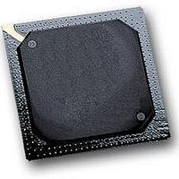
MPC564CZP40 Freescale Semiconductor, MPC564CZP40 Datasheet - Page 617

MPC564CZP40
Manufacturer Part Number
MPC564CZP40
Description
IC MPU 32BIT W/CODE COMP 388PBGA
Manufacturer
Freescale Semiconductor
Series
MPC5xxr
Specifications of MPC564CZP40
Core Processor
PowerPC
Core Size
32-Bit
Speed
40MHz
Connectivity
CAN, EBI/EMI, SCI, SPI, UART/USART
Peripherals
POR, PWM, WDT
Number Of I /o
56
Program Memory Size
512KB (512K x 8)
Program Memory Type
FLASH
Ram Size
32K x 8
Voltage - Supply (vcc/vdd)
2.5 V ~ 2.7 V
Data Converters
A/D 32x10b
Oscillator Type
External
Operating Temperature
-40°C ~ 85°C
Package / Case
388-BGA
Processor Series
MPC5xx
Core
PowerPC
Data Bus Width
32 bit
Data Ram Size
32 KB
Interface Type
CAN, JTAG, QSPI, SCI, SPI, UART
Maximum Clock Frequency
40 MHz
Number Of Programmable I/os
56
Number Of Timers
2
Operating Supply Voltage
0 V to 5 V
Maximum Operating Temperature
+ 85 C
Mounting Style
SMD/SMT
Minimum Operating Temperature
- 40 C
On-chip Adc
2 (10 bit, 32 Channel)
For Use With
MPC564EVB - KIT EVAL FOR MPC561/562/563/564
Lead Free Status / RoHS Status
Contains lead / RoHS non-compliant
Eeprom Size
-
Lead Free Status / Rohs Status
No
Available stocks
Company
Part Number
Manufacturer
Quantity
Price
Company:
Part Number:
MPC564CZP40
Manufacturer:
Freescale Semiconductor
Quantity:
10 000
- Current page: 617 of 1420
- Download datasheet (11Mb)
The current into the signal (I
equations:
where:
The current into (I
parasitic bipolar transistor (K
where I
A method for minimizing the impact of stress conditions on the QADC64E is to strategically allocate
QADC64E inputs so that the lower accuracy inputs are adjacent to the inputs most likely to see stress
conditions.
Also, suitable source impedances should be selected to meet design goals and minimize the effect of stress
conditions.
Freescale Semiconductor
INJ
is either I
I
IN
V
V
(refer to V
V
(refer to V
R
(10-kΩ resistor in
R
= - K
STRESS
SELECTED
STRESS
EB
BE
IN
N
= Parasitic NPN base/emitter voltage
= Parasitic PNP emitter/base voltage
INJN
) the neighboring signal is determined by the K
* I
INJ
= Source impedance
= Adjustable voltage source
or I
NEGCLAMP
NEGCLAMP
Figure 14-53. Input Signal Subjected to Positive Stress
= Source impedance on channel selected for conversion
V
INJP
IN
INJN
N
V
.
<< 1). The I
STRESS
or I
MPC561/MPC563 Reference Manual, Rev. 1.2
Figure 14-52
I INJP
in
in
+
I INJN
INJP
Appendix F, “Electrical
Appendix F, “Electrical
) under negative or positive stress is determined by the following
=
=
R
R
V STRESS V EB
--------------------------------------------------------------------- -
–
----------------------------------------------------- -
SELECTED
IN
STRESS
(
10K
V STRESS V BE
can be expressed by the following equation:
and
R STRESS
R STRESS
I
INJP
I
IN
Figure 14-53
–
PARASITIC
–
AN
AN
DEVICE
n+1
n
–
V DDA
)
Signal Under
Adjacent
Signal
Characteristics”)
Characteristics”))
Stress
on stressed channel)
N
(current coupling ratio) of the
V
DDA
QADC64E Enhanced Mode Operation
QADC64E PAR
Eqn. 14-1
Eqn. 14-2
14-75
Related parts for MPC564CZP40
Image
Part Number
Description
Manufacturer
Datasheet
Request
R

Part Number:
Description:
MPC5 1K0 5%
Manufacturer:
TE Connectivity
Datasheet:

Part Number:
Description:
MPC5 500R 5%
Manufacturer:
TE Connectivity
Datasheet:

Part Number:
Description:
MPC5 5K0 5%
Manufacturer:
Tyco Electronics
Datasheet:

Part Number:
Description:
MPC5 5R0 5%
Manufacturer:
Tyco Electronics
Datasheet:

Part Number:
Description:
MPC5 50K 5%
Manufacturer:
Tyco Electronics
Datasheet:

Part Number:
Description:
MPC5 1R0 5%
Manufacturer:
Tyco Electronics
Datasheet:
Part Number:
Description:
Manufacturer:
Freescale Semiconductor, Inc
Datasheet:
Part Number:
Description:
Manufacturer:
Freescale Semiconductor, Inc
Datasheet:
Part Number:
Description:
Manufacturer:
Freescale Semiconductor, Inc
Datasheet:
Part Number:
Description:
Manufacturer:
Freescale Semiconductor, Inc
Datasheet:
Part Number:
Description:
Manufacturer:
Freescale Semiconductor, Inc
Datasheet:


