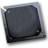
MPC564CZP40 Freescale Semiconductor, MPC564CZP40 Datasheet - Page 1213

MPC564CZP40
Manufacturer Part Number
MPC564CZP40
Description
IC MPU 32BIT W/CODE COMP 388PBGA
Manufacturer
Freescale Semiconductor
Series
MPC5xxr
Specifications of MPC564CZP40
Core Processor
PowerPC
Core Size
32-Bit
Speed
40MHz
Connectivity
CAN, EBI/EMI, SCI, SPI, UART/USART
Peripherals
POR, PWM, WDT
Number Of I /o
56
Program Memory Size
512KB (512K x 8)
Program Memory Type
FLASH
Ram Size
32K x 8
Voltage - Supply (vcc/vdd)
2.5 V ~ 2.7 V
Data Converters
A/D 32x10b
Oscillator Type
External
Operating Temperature
-40°C ~ 85°C
Package / Case
388-BGA
Processor Series
MPC5xx
Core
PowerPC
Data Bus Width
32 bit
Data Ram Size
32 KB
Interface Type
CAN, JTAG, QSPI, SCI, SPI, UART
Maximum Clock Frequency
40 MHz
Number Of Programmable I/os
56
Number Of Timers
2
Operating Supply Voltage
0 V to 5 V
Maximum Operating Temperature
+ 85 C
Mounting Style
SMD/SMT
Minimum Operating Temperature
- 40 C
On-chip Adc
2 (10 bit, 32 Channel)
For Use With
MPC564EVB - KIT EVAL FOR MPC561/562/563/564
Lead Free Status / RoHS Status
Contains lead / RoHS non-compliant
Eeprom Size
-
Lead Free Status / Rohs Status
No
Available stocks
Company
Part Number
Manufacturer
Quantity
Price
Company:
Part Number:
MPC564CZP40
Manufacturer:
Freescale Semiconductor
Quantity:
10 000
- Current page: 1213 of 1420
- Download datasheet (11Mb)
Appendix E
Memory Access Timing
Table E-1
clock values show the number of clocks from the moment an address is valid on a specific bus, until data
is back on that same bus. The following assumptions were used when compiling the information:
Freescale Semiconductor
1
2
3
4
5
RCPU Load/Store
RCPU Instruction Fetches
Peripheral Mode
(only external master is
active)
Slave Mode
(both external and
internal CPUs are active)
•
•
•
•
N is the number of read cycle clocks from external address valid till external data valid. In the case of zero wait states, N
= 2.
Assuming BBC is parked on the U-bus
SIUMCR[BURST_EN] = 1
Until address is valid on external pins
“/” indicates on/off page Flash access.
The arbitration time was ignored. The values assume that the bus (or buses) involved in a
transaction was in the IDLE state when the transaction needs that bus.
The UIMB works in a mode of 1:1. This is relevant for IMB access values. In the case of 2:1 mode,
the clock latency for a cycle on the IMB should be doubled (each IMB access takes two clocks).
The basic delay of an external bus to a U-bus is four clocks (external master case).
All IMB accesses are assumed to be 16-bit accesses only. If 32-bit accesses are used, then each such
IMB access is split into two separate 16-bit cycles with normal IMB performance for each.
lists all possible memory access timings for internal and external memory combinations. The
Table E-1. Memory Access Times Using Different Buses
2-1-1-1-1..
Flash
3/4
4/5
5/6
1
MPC561/MPC563 Reference Manual, Rev. 1.2
RAM
3
1
6
7
Internal Buses
3
DECRA
M
2
6
6
IMB
—
6
7
8
SIU
1
5
6
7
4
External
Memory
Mapped
Internal
External RAM/Flash
4+N
2+N
2
Non-mappe
d Internal
Memory
4+N
2+N
Write Read
Show Cycle
—
2
1
2
5
E-1
Related parts for MPC564CZP40
Image
Part Number
Description
Manufacturer
Datasheet
Request
R

Part Number:
Description:
MPC5 1K0 5%
Manufacturer:
TE Connectivity
Datasheet:

Part Number:
Description:
MPC5 500R 5%
Manufacturer:
TE Connectivity
Datasheet:

Part Number:
Description:
MPC5 5K0 5%
Manufacturer:
Tyco Electronics
Datasheet:

Part Number:
Description:
MPC5 5R0 5%
Manufacturer:
Tyco Electronics
Datasheet:

Part Number:
Description:
MPC5 50K 5%
Manufacturer:
Tyco Electronics
Datasheet:

Part Number:
Description:
MPC5 1R0 5%
Manufacturer:
Tyco Electronics
Datasheet:
Part Number:
Description:
Manufacturer:
Freescale Semiconductor, Inc
Datasheet:
Part Number:
Description:
Manufacturer:
Freescale Semiconductor, Inc
Datasheet:
Part Number:
Description:
Manufacturer:
Freescale Semiconductor, Inc
Datasheet:
Part Number:
Description:
Manufacturer:
Freescale Semiconductor, Inc
Datasheet:
Part Number:
Description:
Manufacturer:
Freescale Semiconductor, Inc
Datasheet:


