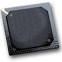
MPC564CZP40 Freescale Semiconductor, MPC564CZP40 Datasheet - Page 224

MPC564CZP40
Manufacturer Part Number
MPC564CZP40
Description
IC MPU 32BIT W/CODE COMP 388PBGA
Manufacturer
Freescale Semiconductor
Series
MPC5xxr
Specifications of MPC564CZP40
Core Processor
PowerPC
Core Size
32-Bit
Speed
40MHz
Connectivity
CAN, EBI/EMI, SCI, SPI, UART/USART
Peripherals
POR, PWM, WDT
Number Of I /o
56
Program Memory Size
512KB (512K x 8)
Program Memory Type
FLASH
Ram Size
32K x 8
Voltage - Supply (vcc/vdd)
2.5 V ~ 2.7 V
Data Converters
A/D 32x10b
Oscillator Type
External
Operating Temperature
-40°C ~ 85°C
Package / Case
388-BGA
Processor Series
MPC5xx
Core
PowerPC
Data Bus Width
32 bit
Data Ram Size
32 KB
Interface Type
CAN, JTAG, QSPI, SCI, SPI, UART
Maximum Clock Frequency
40 MHz
Number Of Programmable I/os
56
Number Of Timers
2
Operating Supply Voltage
0 V to 5 V
Maximum Operating Temperature
+ 85 C
Mounting Style
SMD/SMT
Minimum Operating Temperature
- 40 C
On-chip Adc
2 (10 bit, 32 Channel)
For Use With
MPC564EVB - KIT EVAL FOR MPC561/562/563/564
Lead Free Status / RoHS Status
Contains lead / RoHS non-compliant
Eeprom Size
-
Lead Free Status / Rohs Status
No
Available stocks
Company
Part Number
Manufacturer
Quantity
Price
Company:
Part Number:
MPC564CZP40
Manufacturer:
Freescale Semiconductor
Quantity:
10 000
- Current page: 224 of 1420
- Download datasheet (11Mb)
Burst Buffer Controller 2 Module
All the above registers may be accessed in the supervisor mode only. An exception is internally generated
by the RCPU if there is an attempt to access them in user mode. An external master receives a transfer
error acknowledge when attempting to access a register in user mode.
4.6.1.2
The DECRAM occupies addresses from 0x2F 8000 to 0x2F 87FF. The DCCR block occupies addresses
from 0x2F A000 to 0x2F A03F.
The address for non-implemented memory blocks is not acknowledged, and causes an error condition.
4-18
SPR Number
(Decimal)
784
785
786
787
816
817
818
819
DECRAM and DCCR Block
If one of these registers is written within 4 instructions of a branch target,
the user application may crash. To prevent this, ensure that any instruction
writing to these registers is preceded by 4 instructions that are not the target
of any branch, and is followed by an isync instruction.
Access (Hex)
Address for
External
0x2180
0x2380
0x2580
0x2780
0x2190
0x2390
0x2590
0x2790
Master
IMPU Region Base Address Register 0 (MI_RBA0). See
descriptions.
IMPU Region Base Address Register 1 (MI_RBA1). See
descriptions.
IMPU Region Base Address Register 2 (MI_RBA2). See
descriptions.
IMPU Region Base Address Register 3 (MI_RBA3). See
descriptions.
IMPU Region Attribute Register 0 (MI_RA0). See
IMPU Region Attribute Register 1 (MI_RA1). See
IMPU Region Attribute Register 2 (MI_RA2). See
IMPU Region Attribute Register 3 (MI_RA3). See
MPC561/MPC563 Reference Manual, Rev. 1.2
Table 4-3. BBC SPRs (continued)
NOTE
Register Name
Table 4-6
Table 4-6
Table 4-6
Table 4-6
Table 4-5
Table 4-5
Table 4-5
Table 4-5
for bits descriptions.
for bits descriptions.
for bits descriptions.
for bits descriptions.
Freescale Semiconductor
for bits
for bits
for bits
for bits
Related parts for MPC564CZP40
Image
Part Number
Description
Manufacturer
Datasheet
Request
R

Part Number:
Description:
MPC5 1K0 5%
Manufacturer:
TE Connectivity
Datasheet:

Part Number:
Description:
MPC5 500R 5%
Manufacturer:
TE Connectivity
Datasheet:

Part Number:
Description:
MPC5 5K0 5%
Manufacturer:
Tyco Electronics
Datasheet:

Part Number:
Description:
MPC5 5R0 5%
Manufacturer:
Tyco Electronics
Datasheet:

Part Number:
Description:
MPC5 50K 5%
Manufacturer:
Tyco Electronics
Datasheet:

Part Number:
Description:
MPC5 1R0 5%
Manufacturer:
Tyco Electronics
Datasheet:
Part Number:
Description:
Manufacturer:
Freescale Semiconductor, Inc
Datasheet:
Part Number:
Description:
Manufacturer:
Freescale Semiconductor, Inc
Datasheet:
Part Number:
Description:
Manufacturer:
Freescale Semiconductor, Inc
Datasheet:
Part Number:
Description:
Manufacturer:
Freescale Semiconductor, Inc
Datasheet:
Part Number:
Description:
Manufacturer:
Freescale Semiconductor, Inc
Datasheet:


