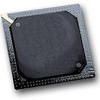
MPC564CZP40 Freescale Semiconductor, MPC564CZP40 Datasheet - Page 913

MPC564CZP40
Manufacturer Part Number
MPC564CZP40
Description
IC MPU 32BIT W/CODE COMP 388PBGA
Manufacturer
Freescale Semiconductor
Series
MPC5xxr
Specifications of MPC564CZP40
Core Processor
PowerPC
Core Size
32-Bit
Speed
40MHz
Connectivity
CAN, EBI/EMI, SCI, SPI, UART/USART
Peripherals
POR, PWM, WDT
Number Of I /o
56
Program Memory Size
512KB (512K x 8)
Program Memory Type
FLASH
Ram Size
32K x 8
Voltage - Supply (vcc/vdd)
2.5 V ~ 2.7 V
Data Converters
A/D 32x10b
Oscillator Type
External
Operating Temperature
-40°C ~ 85°C
Package / Case
388-BGA
Processor Series
MPC5xx
Core
PowerPC
Data Bus Width
32 bit
Data Ram Size
32 KB
Interface Type
CAN, JTAG, QSPI, SCI, SPI, UART
Maximum Clock Frequency
40 MHz
Number Of Programmable I/os
56
Number Of Timers
2
Operating Supply Voltage
0 V to 5 V
Maximum Operating Temperature
+ 85 C
Mounting Style
SMD/SMT
Minimum Operating Temperature
- 40 C
On-chip Adc
2 (10 bit, 32 Channel)
For Use With
MPC564EVB - KIT EVAL FOR MPC561/562/563/564
Lead Free Status / RoHS Status
Contains lead / RoHS non-compliant
Eeprom Size
-
Lead Free Status / Rohs Status
No
Available stocks
Company
Part Number
Manufacturer
Quantity
Price
Company:
Part Number:
MPC564CZP40
Manufacturer:
Freescale Semiconductor
Quantity:
10 000
- Current page: 913 of 1420
- Download datasheet (11Mb)
22.5.3
22.5.4
This register is provided to support a separate module called READI. Refer to
Module.”
The reads from this register will return 0’s.
Freescale Semiconductor
SRESET
SRESET
Bits
3:31
Field OVL DERR CLPS
Field
Addr
0
1
2
CALRAM Overlay Configuration Register (CRAM_OVLCR)
CALRAM Ownership Trace Register (CRAM_OTR)
MSB
16
0
DERR
Name
CLPS
OVL
CRAM_OTR is also defined as READI_OTR. See
“User-Mapped Register
—
Figure 22-11. CALRAM Overlay Configuration Register (CRAM_OVLCR)
17
1
Overlay enable — When set, the CALRAM overlay mode operation is enabled. In this mode
CALRAM allows eight programmable sections (four to 512 bytes) of the on-chip U-bus Flash
memory module to be overlaid by sections of the CALRAM.
0 CALRAM module overlay is disabled
1 CALRAM module overlay is enabled
Data error
0 CALRAM module will not generate machine check exception due to normal L-bus array
1 CALRAM module will generate machine check exception due to normal L-bus array access to
Collapse the total overlay region from 4 Kbytes to 32 bytes; that is, the size is forced to be four
bytes for each for the eight regions regardless of the values programmed in CRAM_RBAx[0:3];
these bits are also referred to as RGN_SIZE[0:3].
0 Overlay region of four Kbytes; region size as specified by CRAM_RBAx[0:3].
1 Overlay region of 32 bytes; each region size is four bytes long regardless of the values in
Reserved
access to the enabled portion overlay region even if overlay is enabled
the enabled portion of overlay region even if overlay is enabled
CRAM_RBAx[0:3].
18
2
19
Table 22-7. CRAMOVLCR Bit Descriptions
3
MPC561/MPC563 Reference Manual, Rev. 1.2
20
4
(OTR).”
21
5
0000_0000_0000_0000
0000_0000_0000_0000
22
6
NOTE
0x38 0028
23
7
—
Description
24
8
—
25
9
Section 24.6.1.1,
10
26
11
27
Chapter 24, “READI
12
28
13
29
CALRAM Operation
14
30
LSB
15
31
22-17
Related parts for MPC564CZP40
Image
Part Number
Description
Manufacturer
Datasheet
Request
R

Part Number:
Description:
MPC5 1K0 5%
Manufacturer:
TE Connectivity
Datasheet:

Part Number:
Description:
MPC5 500R 5%
Manufacturer:
TE Connectivity
Datasheet:

Part Number:
Description:
MPC5 5K0 5%
Manufacturer:
Tyco Electronics
Datasheet:

Part Number:
Description:
MPC5 5R0 5%
Manufacturer:
Tyco Electronics
Datasheet:

Part Number:
Description:
MPC5 50K 5%
Manufacturer:
Tyco Electronics
Datasheet:

Part Number:
Description:
MPC5 1R0 5%
Manufacturer:
Tyco Electronics
Datasheet:
Part Number:
Description:
Manufacturer:
Freescale Semiconductor, Inc
Datasheet:
Part Number:
Description:
Manufacturer:
Freescale Semiconductor, Inc
Datasheet:
Part Number:
Description:
Manufacturer:
Freescale Semiconductor, Inc
Datasheet:
Part Number:
Description:
Manufacturer:
Freescale Semiconductor, Inc
Datasheet:
Part Number:
Description:
Manufacturer:
Freescale Semiconductor, Inc
Datasheet:


