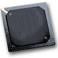
MPC564CZP40 Freescale Semiconductor, MPC564CZP40 Datasheet - Page 499

MPC564CZP40
Manufacturer Part Number
MPC564CZP40
Description
IC MPU 32BIT W/CODE COMP 388PBGA
Manufacturer
Freescale Semiconductor
Series
MPC5xxr
Specifications of MPC564CZP40
Core Processor
PowerPC
Core Size
32-Bit
Speed
40MHz
Connectivity
CAN, EBI/EMI, SCI, SPI, UART/USART
Peripherals
POR, PWM, WDT
Number Of I /o
56
Program Memory Size
512KB (512K x 8)
Program Memory Type
FLASH
Ram Size
32K x 8
Voltage - Supply (vcc/vdd)
2.5 V ~ 2.7 V
Data Converters
A/D 32x10b
Oscillator Type
External
Operating Temperature
-40°C ~ 85°C
Package / Case
388-BGA
Processor Series
MPC5xx
Core
PowerPC
Data Bus Width
32 bit
Data Ram Size
32 KB
Interface Type
CAN, JTAG, QSPI, SCI, SPI, UART
Maximum Clock Frequency
40 MHz
Number Of Programmable I/os
56
Number Of Timers
2
Operating Supply Voltage
0 V to 5 V
Maximum Operating Temperature
+ 85 C
Mounting Style
SMD/SMT
Minimum Operating Temperature
- 40 C
On-chip Adc
2 (10 bit, 32 Channel)
For Use With
MPC564EVB - KIT EVAL FOR MPC561/562/563/564
Lead Free Status / RoHS Status
Contains lead / RoHS non-compliant
Eeprom Size
-
Lead Free Status / Rohs Status
No
Available stocks
Company
Part Number
Manufacturer
Quantity
Price
Company:
Part Number:
MPC564CZP40
Manufacturer:
Freescale Semiconductor
Quantity:
10 000
- Current page: 499 of 1420
- Download datasheet (11Mb)
13.4.1.1
Total conversion time is made up of initial sample time, final sample time, and resolution time. Initial
sample time refers to the time during which the selected input channel is coupled through the buffer
amplifier to the sample capacitor. This buffer is used to quickly reproduce its input signal on the sample
capacitor and minimize charge sharing errors. During the final sampling period the amplifier is bypassed,
and the multiplexer input charges the sample capacitor array directly for improved accuracy. During the
resolution period, the voltage in the sample capacitor is converted to a digital value and stored in the SAR.
Initial sample time is fixed at two QCLK cycles. Final sample time can be 2, 4, 6, 8, or 16 QCLK cycles,
depending on the value of the IST field in the CCW. Resolution time is ten QCLK cycles.
Therefore, conversion time requires a minimum of 14 QCLK clocks (7 µs with a 2.0-MHz QCLK). If the
maximum final sample time period of 16 QCLKs is selected, the total conversion time is 28 QCLKs or 14
µs (with a 2.0-MHz QCLK)
Figure 13-21
13.4.1.2
If the amplifier bypass mode is enabled for a conversion by setting the amplifier bypass (BYP) bit in the
CCW, the timing changes to that shown in
the potential conversion time by two QCLKs. However, due to internal RC effects, a minimum final
sample time of four QCLKs must be allowed. This results in no savings of QCLKs. When using the bypass
mode, the external circuit should be of low source impedance, typically less than 10 kΩ. Also, the loading
effects of the external circuitry by the QADC64E need to be considered, since the benefits of the sample
amplifier are not present.
Freescale Semiconductor
QCLK
Conversion Cycle Times
Amplifier Bypass Mode Conversion Timing
illustrates the timing for conversions.
Because of internal RC time constants, a sample time of two QCLKs in
bypass mode for high frequency operation is not recommended.
2 cycles
Sample
BUFFER
Time
Sample TIME
Final Sample
(2, 4, 8, 16)
N cycles:
MPC561/MPC563 Reference Manual, Rev. 1.2
Time
Figure 13-21. Conversion Timing
Figure
Successive Approximation Resolution
13-22. The buffered sample time is eliminated, reducing
NOTE
Sequence
Resolution
10 cycles
Time
QADC64E Legacy Mode Operation
13-35
Related parts for MPC564CZP40
Image
Part Number
Description
Manufacturer
Datasheet
Request
R

Part Number:
Description:
MPC5 1K0 5%
Manufacturer:
TE Connectivity
Datasheet:

Part Number:
Description:
MPC5 500R 5%
Manufacturer:
TE Connectivity
Datasheet:

Part Number:
Description:
MPC5 5K0 5%
Manufacturer:
Tyco Electronics
Datasheet:

Part Number:
Description:
MPC5 5R0 5%
Manufacturer:
Tyco Electronics
Datasheet:

Part Number:
Description:
MPC5 50K 5%
Manufacturer:
Tyco Electronics
Datasheet:

Part Number:
Description:
MPC5 1R0 5%
Manufacturer:
Tyco Electronics
Datasheet:
Part Number:
Description:
Manufacturer:
Freescale Semiconductor, Inc
Datasheet:
Part Number:
Description:
Manufacturer:
Freescale Semiconductor, Inc
Datasheet:
Part Number:
Description:
Manufacturer:
Freescale Semiconductor, Inc
Datasheet:
Part Number:
Description:
Manufacturer:
Freescale Semiconductor, Inc
Datasheet:
Part Number:
Description:
Manufacturer:
Freescale Semiconductor, Inc
Datasheet:


