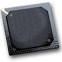
MPC564CZP40 Freescale Semiconductor, MPC564CZP40 Datasheet - Page 949

MPC564CZP40
Manufacturer Part Number
MPC564CZP40
Description
IC MPU 32BIT W/CODE COMP 388PBGA
Manufacturer
Freescale Semiconductor
Series
MPC5xxr
Specifications of MPC564CZP40
Core Processor
PowerPC
Core Size
32-Bit
Speed
40MHz
Connectivity
CAN, EBI/EMI, SCI, SPI, UART/USART
Peripherals
POR, PWM, WDT
Number Of I /o
56
Program Memory Size
512KB (512K x 8)
Program Memory Type
FLASH
Ram Size
32K x 8
Voltage - Supply (vcc/vdd)
2.5 V ~ 2.7 V
Data Converters
A/D 32x10b
Oscillator Type
External
Operating Temperature
-40°C ~ 85°C
Package / Case
388-BGA
Processor Series
MPC5xx
Core
PowerPC
Data Bus Width
32 bit
Data Ram Size
32 KB
Interface Type
CAN, JTAG, QSPI, SCI, SPI, UART
Maximum Clock Frequency
40 MHz
Number Of Programmable I/os
56
Number Of Timers
2
Operating Supply Voltage
0 V to 5 V
Maximum Operating Temperature
+ 85 C
Mounting Style
SMD/SMT
Minimum Operating Temperature
- 40 C
On-chip Adc
2 (10 bit, 32 Channel)
For Use With
MPC564EVB - KIT EVAL FOR MPC561/562/563/564
Lead Free Status / RoHS Status
Contains lead / RoHS non-compliant
Eeprom Size
-
Lead Free Status / Rohs Status
No
Available stocks
Company
Part Number
Manufacturer
Quantity
Price
Company:
Part Number:
MPC564CZP40
Manufacturer:
Freescale Semiconductor
Quantity:
10 000
- Current page: 949 of 1420
- Download datasheet (11Mb)
When not in debug mode the sequencing error encoding indicates that the transmission from the external
development tool was a debug mode transmission. When a sequencing error occurs the development port
will ignore the data shifted in while the sequencing error was shifting out. It will be treated as a NOP
function.
Finally, the null output encoding is used to indicate that the previous transmission did not have any
associated errors.
When not in debug mode, ready will be asserted at the end of each transmission. If debug mode is not
enabled and transmission errors can be guaranteed not to occur, the status output is not needed.
23.4.6.8
When in debug mode the development port starts communications by setting DSDO low to indicate that
the CPU is trying to read an instruction from DPIR or data from DPDR. When the CPU writes data to the
port to be shifted out the ready bit is not set. The port waits for the CPU to read the next instruction before
asserting ready. This allows duplex operation of the serial port while allowing the port to control all
transmissions from the external development tool. After detecting this ready status the external
development tool begins the transmission to the development port with a start bit (logic high) on the DSDI
pin.
23.4.6.9
mode/status bit, a control/status bit, and 32 bits of data. All instructions and data for the CPU are
transmitted with the mode bit cleared indicating a 32-bit data field. The encoding of data shifted into the
development port shift register (through the DSDI pin) is shown below in
Freescale Semiconductor
In debug mode the 35 bits of the development port shift register are interpreted as a start/ready bit, a
1
2
Ready
The “Freeze” status is set to (1) when the CPU is in debug mode and to (0) otherwise.
The “Download Procedure in progress” status is asserted (0) when Debug port in the Download procedure and is
negated (1) otherwise.
(0)
(0)
(0)
(0)
Development Port Serial Communications — Debug Mode
Serial Data Into Development Port
Table 23-12. Status / Data Shifted Out of Development Port Shift Register
0
0
1
1
Status [0:1]
0
1
0
1
MPC561/MPC563 Reference Manual, Rev. 1.2
Freeze
status
Bit 0
1
Procedure
Download
progress
Bit 1
in
2
Data
Data
(Depending on Input Mode)
Bits 2:31 or 2:6 —
1’s
1’s
1’s
Table
23-13.
Valid Data from CPU
Sequencing Error
CPU Interrupt
Null
Function
Development Support
23-35
Related parts for MPC564CZP40
Image
Part Number
Description
Manufacturer
Datasheet
Request
R

Part Number:
Description:
MPC5 1K0 5%
Manufacturer:
TE Connectivity
Datasheet:

Part Number:
Description:
MPC5 500R 5%
Manufacturer:
TE Connectivity
Datasheet:

Part Number:
Description:
MPC5 5K0 5%
Manufacturer:
Tyco Electronics
Datasheet:

Part Number:
Description:
MPC5 5R0 5%
Manufacturer:
Tyco Electronics
Datasheet:

Part Number:
Description:
MPC5 50K 5%
Manufacturer:
Tyco Electronics
Datasheet:

Part Number:
Description:
MPC5 1R0 5%
Manufacturer:
Tyco Electronics
Datasheet:
Part Number:
Description:
Manufacturer:
Freescale Semiconductor, Inc
Datasheet:
Part Number:
Description:
Manufacturer:
Freescale Semiconductor, Inc
Datasheet:
Part Number:
Description:
Manufacturer:
Freescale Semiconductor, Inc
Datasheet:
Part Number:
Description:
Manufacturer:
Freescale Semiconductor, Inc
Datasheet:
Part Number:
Description:
Manufacturer:
Freescale Semiconductor, Inc
Datasheet:


