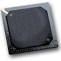
MPC564CZP40 Freescale Semiconductor, MPC564CZP40 Datasheet - Page 908

MPC564CZP40
Manufacturer Part Number
MPC564CZP40
Description
IC MPU 32BIT W/CODE COMP 388PBGA
Manufacturer
Freescale Semiconductor
Series
MPC5xxr
Specifications of MPC564CZP40
Core Processor
PowerPC
Core Size
32-Bit
Speed
40MHz
Connectivity
CAN, EBI/EMI, SCI, SPI, UART/USART
Peripherals
POR, PWM, WDT
Number Of I /o
56
Program Memory Size
512KB (512K x 8)
Program Memory Type
FLASH
Ram Size
32K x 8
Voltage - Supply (vcc/vdd)
2.5 V ~ 2.7 V
Data Converters
A/D 32x10b
Oscillator Type
External
Operating Temperature
-40°C ~ 85°C
Package / Case
388-BGA
Processor Series
MPC5xx
Core
PowerPC
Data Bus Width
32 bit
Data Ram Size
32 KB
Interface Type
CAN, JTAG, QSPI, SCI, SPI, UART
Maximum Clock Frequency
40 MHz
Number Of Programmable I/os
56
Number Of Timers
2
Operating Supply Voltage
0 V to 5 V
Maximum Operating Temperature
+ 85 C
Mounting Style
SMD/SMT
Minimum Operating Temperature
- 40 C
On-chip Adc
2 (10 bit, 32 Channel)
For Use With
MPC564EVB - KIT EVAL FOR MPC561/562/563/564
Lead Free Status / RoHS Status
Contains lead / RoHS non-compliant
Eeprom Size
-
Lead Free Status / Rohs Status
No
Available stocks
Company
Part Number
Manufacturer
Quantity
Price
Company:
Part Number:
MPC564CZP40
Manufacturer:
Freescale Semiconductor
Quantity:
10 000
- Current page: 908 of 1420
- Download datasheet (11Mb)
CALRAM Operation
22.4.6.3
If overlay is enabled and CRAMOVLCR[DERR] is set, then any normal L-bus array access that falls
within any of the eight enabled overlay regions generates a machine-check exception; otherwise the access
terminates normally without asserting data error. The L-bus write accesses cause the data to be written
regardless of whether the DERR bit is set or not.
For example, if overlay region 1 is programmed such that it is enabled and its region size is 256 bytes, then
any L-bus access to address in the range of 0x3F F200 – 0x3F F2FF generates machine check exception
if the DERR bit is set in CRAMOVLCR register. The other portion of region 1 from 0x3F F300 to 0x3F
F3FF can be used as normal (non-overlay) array.
22.4.6.4
Write accesses to the overlaid U-bus Flash regions are ignored completely by the CALRAM module.
22.5
The following section describes the CALRAM programmer’s model. The CALRAM has one register
(CRAMMCR) for configuring the CALRAM array and one register dedicated to factory test. In addition,
there are eight 32-bit region base address registers for calibration purposes and a 32-bit overlay
configuration register. The region base address registers hold the base address for the Flash region and
region size that need to be overlaid by the CALRAM. The overlay configuration register provides three
bits (OVL, DERR, and CLSP) that are needed for overlay configuration. The CALRAM ownership trace
register (CRAM_OTR) is provided to support a separate module called a READI module. Access to all
CALRAM registers requires the bus master to be in supervisor data mode. On a privilege violation, the
register is not accessed and the access generates an error.
Table 22-2
22-12
minimal amount of reprogramming efforts.
Programming Model
shows the register address map for the MPC561/MPC563.
Normal (Non-Overlay) Access to Overlay Regions
Calibration Write Cycle Flow
Module/Region Number
CALRAM/region 0
CALRAM/region 1
CALRAM/region 2
CALRAM/region 3
CALRAM/region 4
CALRAM/region 5
CALRAM/region 6
CALRAM/region 7
Table 22-1. Priorities of Overlay Regions
MPC561/MPC563 Reference Manual, Rev. 1.2
Priority
Highest
Lowest
.
.
.
.
.
.
Freescale Semiconductor
Related parts for MPC564CZP40
Image
Part Number
Description
Manufacturer
Datasheet
Request
R

Part Number:
Description:
MPC5 1K0 5%
Manufacturer:
TE Connectivity
Datasheet:

Part Number:
Description:
MPC5 500R 5%
Manufacturer:
TE Connectivity
Datasheet:

Part Number:
Description:
MPC5 5K0 5%
Manufacturer:
Tyco Electronics
Datasheet:

Part Number:
Description:
MPC5 5R0 5%
Manufacturer:
Tyco Electronics
Datasheet:

Part Number:
Description:
MPC5 50K 5%
Manufacturer:
Tyco Electronics
Datasheet:

Part Number:
Description:
MPC5 1R0 5%
Manufacturer:
Tyco Electronics
Datasheet:
Part Number:
Description:
Manufacturer:
Freescale Semiconductor, Inc
Datasheet:
Part Number:
Description:
Manufacturer:
Freescale Semiconductor, Inc
Datasheet:
Part Number:
Description:
Manufacturer:
Freescale Semiconductor, Inc
Datasheet:
Part Number:
Description:
Manufacturer:
Freescale Semiconductor, Inc
Datasheet:
Part Number:
Description:
Manufacturer:
Freescale Semiconductor, Inc
Datasheet:


