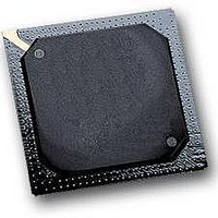
MPC564CZP40 Freescale Semiconductor, MPC564CZP40 Datasheet - Page 437

MPC564CZP40
Manufacturer Part Number
MPC564CZP40
Description
IC MPU 32BIT W/CODE COMP 388PBGA
Manufacturer
Freescale Semiconductor
Series
MPC5xxr
Specifications of MPC564CZP40
Core Processor
PowerPC
Core Size
32-Bit
Speed
40MHz
Connectivity
CAN, EBI/EMI, SCI, SPI, UART/USART
Peripherals
POR, PWM, WDT
Number Of I /o
56
Program Memory Size
512KB (512K x 8)
Program Memory Type
FLASH
Ram Size
32K x 8
Voltage - Supply (vcc/vdd)
2.5 V ~ 2.7 V
Data Converters
A/D 32x10b
Oscillator Type
External
Operating Temperature
-40°C ~ 85°C
Package / Case
388-BGA
Processor Series
MPC5xx
Core
PowerPC
Data Bus Width
32 bit
Data Ram Size
32 KB
Interface Type
CAN, JTAG, QSPI, SCI, SPI, UART
Maximum Clock Frequency
40 MHz
Number Of Programmable I/os
56
Number Of Timers
2
Operating Supply Voltage
0 V to 5 V
Maximum Operating Temperature
+ 85 C
Mounting Style
SMD/SMT
Minimum Operating Temperature
- 40 C
On-chip Adc
2 (10 bit, 32 Channel)
For Use With
MPC564EVB - KIT EVAL FOR MPC561/562/563/564
Lead Free Status / RoHS Status
Contains lead / RoHS non-compliant
Eeprom Size
-
Lead Free Status / Rohs Status
No
Available stocks
Company
Part Number
Manufacturer
Quantity
Price
Company:
Part Number:
MPC564CZP40
Manufacturer:
Freescale Semiconductor
Quantity:
10 000
- Current page: 437 of 1420
- Download datasheet (11Mb)
Chapter 11
L-Bus to U-Bus Interface (L2U)
The L-bus to U-bus interface unit (L2U) provides an interface between the load/store bus (L-bus) and the
unified bus (U-bus). The L2U module includes the data memory protection unit (DMPU), which provides
protection for data memory accesses.
The L2U is bidirectional. It allows load/store accesses not intended for the L-bus data RAM to go to the
U-bus. It also allows code execution from the L-bus data RAM and read/write accesses from the U-bus to
the L-bus.
The L2U directs bus traffic between the L-bus and the U-bus. When transactions start concurrently on both
buses, the L2U interface arbitrates to select which transaction is handled. The top priority is assigned to
U-bus to L-bus accesses; lower priority is assigned to the load/store accesses by the RCPU.
11.1
11.2
Freescale Semiconductor
•
•
•
•
•
•
•
•
Non-pipelined master and slave on U-bus
— Does not start two back-to-back accesses on the U-bus
— Supports U-bus pipelining
— Retries back-to-back accesses from U-bus masters
Non-pipelined master and slave on the L-bus
Generates module selects for L-bus memory-mapped resources within a programmable,
contiguous block of storage
Programmable data memory protection unit (DMPU)
L-bus and U-bus snoop logic for the reservation protocol compatible with the PowerPC ISA
architecture
Show cycles for RCPU accesses to the CALRAM (none, all, writes)
— Protection for CALRAM accesses from the U-bus side (all accesses to the CALRAM from the
Supports four memory regions whose base address and size can be programmed
— Available sizes are 4 Kbytes, 8 Kbytes, 16 Kbytes, 32 Kbytes, 64 Kbytes, 128 Kbytes, 256
— Region must start on the specified region size boundary (modulo addressing)
— Overlap between regions is allowed
Each of the four regions supports the following attributes:
General Features
Data Memory Protection Unit Features
U-bus side are blocked once the CALRAM protection bit is set)
Kbytes, 512 Kbytes, 1 Mbyte, 2 Mbytes, 4 Mbytes, 8 Mbytes, and 16 Mybtes
MPC561/MPC563 Reference Manual, Rev. 1.2
11-1
Related parts for MPC564CZP40
Image
Part Number
Description
Manufacturer
Datasheet
Request
R

Part Number:
Description:
MPC5 1K0 5%
Manufacturer:
TE Connectivity
Datasheet:

Part Number:
Description:
MPC5 500R 5%
Manufacturer:
TE Connectivity
Datasheet:

Part Number:
Description:
MPC5 5K0 5%
Manufacturer:
Tyco Electronics
Datasheet:

Part Number:
Description:
MPC5 5R0 5%
Manufacturer:
Tyco Electronics
Datasheet:

Part Number:
Description:
MPC5 50K 5%
Manufacturer:
Tyco Electronics
Datasheet:

Part Number:
Description:
MPC5 1R0 5%
Manufacturer:
Tyco Electronics
Datasheet:
Part Number:
Description:
Manufacturer:
Freescale Semiconductor, Inc
Datasheet:
Part Number:
Description:
Manufacturer:
Freescale Semiconductor, Inc
Datasheet:
Part Number:
Description:
Manufacturer:
Freescale Semiconductor, Inc
Datasheet:
Part Number:
Description:
Manufacturer:
Freescale Semiconductor, Inc
Datasheet:
Part Number:
Description:
Manufacturer:
Freescale Semiconductor, Inc
Datasheet:


