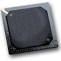
MPC564CZP40 Freescale Semiconductor, MPC564CZP40 Datasheet - Page 234

MPC564CZP40
Manufacturer Part Number
MPC564CZP40
Description
IC MPU 32BIT W/CODE COMP 388PBGA
Manufacturer
Freescale Semiconductor
Series
MPC5xxr
Specifications of MPC564CZP40
Core Processor
PowerPC
Core Size
32-Bit
Speed
40MHz
Connectivity
CAN, EBI/EMI, SCI, SPI, UART/USART
Peripherals
POR, PWM, WDT
Number Of I /o
56
Program Memory Size
512KB (512K x 8)
Program Memory Type
FLASH
Ram Size
32K x 8
Voltage - Supply (vcc/vdd)
2.5 V ~ 2.7 V
Data Converters
A/D 32x10b
Oscillator Type
External
Operating Temperature
-40°C ~ 85°C
Package / Case
388-BGA
Processor Series
MPC5xx
Core
PowerPC
Data Bus Width
32 bit
Data Ram Size
32 KB
Interface Type
CAN, JTAG, QSPI, SCI, SPI, UART
Maximum Clock Frequency
40 MHz
Number Of Programmable I/os
56
Number Of Timers
2
Operating Supply Voltage
0 V to 5 V
Maximum Operating Temperature
+ 85 C
Mounting Style
SMD/SMT
Minimum Operating Temperature
- 40 C
On-chip Adc
2 (10 bit, 32 Channel)
For Use With
MPC564EVB - KIT EVAL FOR MPC561/562/563/564
Lead Free Status / RoHS Status
Contains lead / RoHS non-compliant
Eeprom Size
-
Lead Free Status / Rohs Status
No
Available stocks
Company
Part Number
Manufacturer
Quantity
Price
Company:
Part Number:
MPC564CZP40
Manufacturer:
Freescale Semiconductor
Quantity:
10 000
- Current page: 234 of 1420
- Download datasheet (11Mb)
Unified System Interface Unit (USIU) Overview
The USIU supports the internal Flash censorship mechanism on the MPC561/MPC563 to protect the Flash
contents. Refer to
MPC561/MPC563 from the external world while the Flash is in censorship mode and in a censorship state.
The internal Flash array will be either locked or accessible only after the entire array contents have been
erased. The MPC561/MPC563 is in censored mode if one of the following events occurs:
Figure 5-1
5.1
Table 5-1
The address shown for each register is relative to the base address of the MPC561/MPC563 internal
memory map. The internal memory block can reside in one of eight possible 4 Mbyte memory spaces. See
Figure 1-3
5-2
•
•
•
booting from external memory
operating in peripheral mode or if accessed from an external master
operating in debug mode (BDM or Nexus)
Memory Map and Registers
is an address map of the USIU registers and, unless otherwise noted, registers are 32 bits wide.
shows the USIU block diagram.
for details.
USIU
• Software Watchdog
• Bus Monitor
• Periodic Interrupt
• Timer and Decrementer
• Real-time Clock
• Debug
• Pin Multiplexing
• Interrupt Controller
Configuration Registers
Chapter 21, “CDR3 Flash (UC3F)
U-Bus
MPC561/MPC563 Reference Manual, Rev. 1.2
Interface
U-bus
Figure 5-1. USIU Block Diagram
Interface
Controller
SGPIO
Memory
Slave
EEPROM.” It is not possible to operate the
Address
Data
Memory Control Lines
Clocks & Reset
Interface
E-bus
Freescale Semiconductor
E-Bus
Related parts for MPC564CZP40
Image
Part Number
Description
Manufacturer
Datasheet
Request
R

Part Number:
Description:
MPC5 1K0 5%
Manufacturer:
TE Connectivity
Datasheet:

Part Number:
Description:
MPC5 500R 5%
Manufacturer:
TE Connectivity
Datasheet:

Part Number:
Description:
MPC5 5K0 5%
Manufacturer:
Tyco Electronics
Datasheet:

Part Number:
Description:
MPC5 5R0 5%
Manufacturer:
Tyco Electronics
Datasheet:

Part Number:
Description:
MPC5 50K 5%
Manufacturer:
Tyco Electronics
Datasheet:

Part Number:
Description:
MPC5 1R0 5%
Manufacturer:
Tyco Electronics
Datasheet:
Part Number:
Description:
Manufacturer:
Freescale Semiconductor, Inc
Datasheet:
Part Number:
Description:
Manufacturer:
Freescale Semiconductor, Inc
Datasheet:
Part Number:
Description:
Manufacturer:
Freescale Semiconductor, Inc
Datasheet:
Part Number:
Description:
Manufacturer:
Freescale Semiconductor, Inc
Datasheet:
Part Number:
Description:
Manufacturer:
Freescale Semiconductor, Inc
Datasheet:


