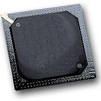
MPC564CZP40 Freescale Semiconductor, MPC564CZP40 Datasheet - Page 865

MPC564CZP40
Manufacturer Part Number
MPC564CZP40
Description
IC MPU 32BIT W/CODE COMP 388PBGA
Manufacturer
Freescale Semiconductor
Series
MPC5xxr
Specifications of MPC564CZP40
Core Processor
PowerPC
Core Size
32-Bit
Speed
40MHz
Connectivity
CAN, EBI/EMI, SCI, SPI, UART/USART
Peripherals
POR, PWM, WDT
Number Of I /o
56
Program Memory Size
512KB (512K x 8)
Program Memory Type
FLASH
Ram Size
32K x 8
Voltage - Supply (vcc/vdd)
2.5 V ~ 2.7 V
Data Converters
A/D 32x10b
Oscillator Type
External
Operating Temperature
-40°C ~ 85°C
Package / Case
388-BGA
Processor Series
MPC5xx
Core
PowerPC
Data Bus Width
32 bit
Data Ram Size
32 KB
Interface Type
CAN, JTAG, QSPI, SCI, SPI, UART
Maximum Clock Frequency
40 MHz
Number Of Programmable I/os
56
Number Of Timers
2
Operating Supply Voltage
0 V to 5 V
Maximum Operating Temperature
+ 85 C
Mounting Style
SMD/SMT
Minimum Operating Temperature
- 40 C
On-chip Adc
2 (10 bit, 32 Channel)
For Use With
MPC564EVB - KIT EVAL FOR MPC561/562/563/564
Lead Free Status / RoHS Status
Contains lead / RoHS non-compliant
Eeprom Size
-
Lead Free Status / Rohs Status
No
Available stocks
Company
Part Number
Manufacturer
Quantity
Price
Company:
Part Number:
MPC564CZP40
Manufacturer:
Freescale Semiconductor
Quantity:
10 000
- Current page: 865 of 1420
- Download datasheet (11Mb)
To prevent unnecessary page accesses from the array, the UC3F memory interface (MI) monitors the
incoming address to determine if the required information is in one of the two read page buffers. This
strategy allows the UC3F array to have an off page access and an on page access. In normal operation,
write accesses to the UC3F array are not recognized except during program and erase operations.
The UC3F EEPROM uses an embedded hardware algorithm to program and erase the UC3F array. Special
control logic is included to guard against accidental program or erase by requiring a specific series of read
and write accesses to the UC3F control registers. External inputs provide a hardware protection
mechanism to prevent accidental program and erase of UC3F array blocks. The hardware algorithm
automatically performs all necessary applications of high voltage pulses and verify reads of the UC3F
array to ensure that all bits are programmed and erased with sufficient margin to guarantee data integrity
and reliability.
21.0.1
Freescale Semiconductor
•
•
•
•
•
•
•
•
•
•
•
•
•
High density single transistor Flash bit cell
-40 to 125° C ambient temperature operating range
— -40 to 85° C on the suffix C device
2.5-V to 2.7-V V
Shadow information stored in special Flash NVM shadow locations
512 Kbytes using 64-Kbyte blocks
— Two 16-Kbyte small blocks
Array block restriction control for small and large blocks
— Erase by array blocks
— Array protection for program and erase operations
— Array block assignment of supervisor or supervisor/user space
— Array block assignment of data or instruction/data space
Internal 64-bit data path architecture
Page mode read
— Retains two independent read page buffers
— Read page size of 32 bytes (8 words).
Word (32-bit) programming
Embedded hardware program and erase algorithm
— Uses internal oscillator to time program and erase pulses. Pulses are timed independently of
— Automatically performs margin reads
External Flash program or erase enable inputs for block 0 or entire Flash array (B0EPEE and
EPEE)
Low power disable via an external signal or UC3F register bit
Censor mode for Flash memory array access restriction with a user bypass for unrestricted array
access
system clock frequency
Features of the CDR3 Flash EEPROM (UC3F)
DDF
operating range and 4.75-V to 5.25-V V
MPC561/MPC563 Reference Manual, Rev. 1.2
FLASH
operating range
CDR3 Flash (UC3F) EEPROM
21-3
Related parts for MPC564CZP40
Image
Part Number
Description
Manufacturer
Datasheet
Request
R

Part Number:
Description:
MPC5 1K0 5%
Manufacturer:
TE Connectivity
Datasheet:

Part Number:
Description:
MPC5 500R 5%
Manufacturer:
TE Connectivity
Datasheet:

Part Number:
Description:
MPC5 5K0 5%
Manufacturer:
Tyco Electronics
Datasheet:

Part Number:
Description:
MPC5 5R0 5%
Manufacturer:
Tyco Electronics
Datasheet:

Part Number:
Description:
MPC5 50K 5%
Manufacturer:
Tyco Electronics
Datasheet:

Part Number:
Description:
MPC5 1R0 5%
Manufacturer:
Tyco Electronics
Datasheet:
Part Number:
Description:
Manufacturer:
Freescale Semiconductor, Inc
Datasheet:
Part Number:
Description:
Manufacturer:
Freescale Semiconductor, Inc
Datasheet:
Part Number:
Description:
Manufacturer:
Freescale Semiconductor, Inc
Datasheet:
Part Number:
Description:
Manufacturer:
Freescale Semiconductor, Inc
Datasheet:
Part Number:
Description:
Manufacturer:
Freescale Semiconductor, Inc
Datasheet:


