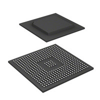
R8A77850ADBGV Renesas Electronics America, R8A77850ADBGV Datasheet - Page 382

R8A77850ADBGV
Manufacturer Part Number
R8A77850ADBGV
Description
IC SUPERH MPU ROMLESS 436-BGA
Manufacturer
Renesas Electronics America
Series
SuperH® SH7780r
Datasheet
1.R8A77850AADBGV.pdf
(1694 pages)
Specifications of R8A77850ADBGV
Core Processor
SH-4A
Core Size
32-Bit
Speed
600MHz
Connectivity
Audio Codec, MMC, Serial Sound, SCI, SIO, SPI, SSI
Peripherals
DMA, POR, WDT
Number Of I /o
108
Program Memory Type
ROMless
Ram Size
8K x 8
Voltage - Supply (vcc/vdd)
1 V ~ 1.2 V
Oscillator Type
External
Operating Temperature
-40°C ~ 85°C
Package / Case
436-BGA
Lead Free Status / RoHS Status
Lead free / RoHS Compliant
Eeprom Size
-
Program Memory Size
-
Data Converters
-
Available stocks
Company
Part Number
Manufacturer
Quantity
Price
Company:
Part Number:
R8A77850ADBGV
Manufacturer:
Renesas Electronics America
Quantity:
10 000
Company:
Part Number:
R8A77850ADBGV#RD0Z
Manufacturer:
Renesas Electronics America
Quantity:
10 000
- Current page: 382 of 1694
- Download datasheet (9Mb)
11. Local Bus State Controller (LBSC)
11.2
Table 11.1 shows the LBSC pin configuration.
Table 11.1 Pin Configuration
Rev.1.00 Jan. 10, 2008 Page 350 of 1658
REJ09B0261-0100
Pin Name
A25 to A0
D63 to D0
BS
CS6 to CS0
R/W
RD/FRAME
Input/Output Pins
Function
Address Bus
Data Bus
Bus Cycle Start O
Chip Select 6 to
0
Read/Write
Read/Cycle
Frame
I/O
O
I/O
O
O
O
Description
Address output
Data input/output
These pins are multiplexed as follows:
D63 to D56: PCI, DU and ports A7 to A0 (GPIO
D55 to D48: PCI, DU and ports B7 to B0 (GPIO
D47 to D40: PCI, DU and ports C7 to C0 (GPIO
D39 to D32: PCI, DU and ports D7 to D0 (GPIO
D31 to D24: ports F7 to F0 (GPIO input/output)
D23 to D16: ports G7 to G0 (GPIO input/output)
Signal that indicates the start of a bus cycle
Asserted once for a burst transfer when the MPX
interface is set
Asserted in every data cycle in other burst
transfers
Chip select signals that indicates the area being
accessed. CS5 and CS6 can also be used as
CE1A and CE1B of the PCMCIA respectively.
Data bus input/output direction designation
signal. Also used as the PCMCIA interface write
designation signal
Strobe signal indicating a read cycle.
Used for FRAME signal when the MPX bus is
used
input/output)
input/output)
input/output)
input/output)
Related parts for R8A77850ADBGV
Image
Part Number
Description
Manufacturer
Datasheet
Request
R

Part Number:
Description:
KIT STARTER FOR M16C/29
Manufacturer:
Renesas Electronics America
Datasheet:

Part Number:
Description:
KIT STARTER FOR R8C/2D
Manufacturer:
Renesas Electronics America
Datasheet:

Part Number:
Description:
R0K33062P STARTER KIT
Manufacturer:
Renesas Electronics America
Datasheet:

Part Number:
Description:
KIT STARTER FOR R8C/23 E8A
Manufacturer:
Renesas Electronics America
Datasheet:

Part Number:
Description:
KIT STARTER FOR R8C/25
Manufacturer:
Renesas Electronics America
Datasheet:

Part Number:
Description:
KIT STARTER H8S2456 SHARPE DSPLY
Manufacturer:
Renesas Electronics America
Datasheet:

Part Number:
Description:
KIT STARTER FOR R8C38C
Manufacturer:
Renesas Electronics America
Datasheet:

Part Number:
Description:
KIT STARTER FOR R8C35C
Manufacturer:
Renesas Electronics America
Datasheet:

Part Number:
Description:
KIT STARTER FOR R8CL3AC+LCD APPS
Manufacturer:
Renesas Electronics America
Datasheet:

Part Number:
Description:
KIT STARTER FOR RX610
Manufacturer:
Renesas Electronics America
Datasheet:

Part Number:
Description:
KIT STARTER FOR R32C/118
Manufacturer:
Renesas Electronics America
Datasheet:

Part Number:
Description:
KIT DEV RSK-R8C/26-29
Manufacturer:
Renesas Electronics America
Datasheet:

Part Number:
Description:
KIT STARTER FOR SH7124
Manufacturer:
Renesas Electronics America
Datasheet:

Part Number:
Description:
KIT STARTER FOR H8SX/1622
Manufacturer:
Renesas Electronics America
Datasheet:

Part Number:
Description:
KIT DEV FOR SH7203
Manufacturer:
Renesas Electronics America
Datasheet:


