IPR-PCIE/1 Altera, IPR-PCIE/1 Datasheet - Page 186
IPR-PCIE/1
Manufacturer Part Number
IPR-PCIE/1
Description
IP CORE Renewal Of IP-PCIE/1
Manufacturer
Altera
Type
MegaCorer
Specifications of IPR-PCIE/1
Software Application
IP CORE, Interface And Protocols, PCI
Supported Families
Arria GX, Cyclone II, HardCopy II, Stratix II
Core Architecture
FPGA
Core Sub-architecture
Arria, Cyclone, Stratix
Rohs Compliant
NA
Function
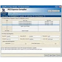
PCI Express Compiler, x1 Link Width
License
Renewal License
Lead Free Status / RoHS Status
na
Lead Free Status / RoHS Status
na


9–4
Table 9–3. L0s and L1 Exit Latency
PCI Express Compiler User Guide
L0s
L1
Power
State
Acceptable Latency
L0s exit latency is calculated by the IP core based on the number of fast training sequences specified on the
Power Management page of the MegaWizard Plug-In Manager. It is maintained in a configuration space
registry. Main power and the reference clock remain present and the PHY should resynchronize quickly for
receive data.
Resynchronization is performed through fast training order sets, which are sent by the connected component.
A component knows how many sets to send because of the initialization process, at which time the required
number of sets is determined through training sequence ordered sets (TS1 and TS2).
L1 exit latency is specified on the Power Management page of the MegaWizard Plug-In Manager. It is
maintained in a configuration space registry. Both components across a link must transition to L1 low-power
state together. When in L1, a component’s PHY is also in P1 low-power state for additional power savings.
Main power and the reference clock are still present, but the PHY can shut down all PLLs to save additional
power. However, shutting down PLLs causes a longer transition time to L0.
L1 exit latency is higher than L0s exit latency. When the transmit PLL is locked, the LTSSM moves to recovery,
and back to L0 after both components have correctly negotiated the recovery state. Thus, the exact L1 exit
latency depends on the exit latency of each component (the higher value of the two components). All
calculations are performed by software; however, each component reports its own L1 exit latency.
■
Each component must report in the configuration space if they use the slot’s reference
clock. Software then programs the common clock register, depending on the reference
clock of each component. Software also retrains the link after changing the common
clock register value to update each exit latency.
latency. Each component maintains two values for L0s and L1 exit latencies; one for
the common clock configuration and the other for the separate clock configuration.
The acceptable latency is defined as the maximum latency permitted for a component
to transition from a low power state to L0 without compromising system
performance. Acceptable latency values depend on a component’s internal buffering
and are maintained in a configuration space registry. Software compares the link exit
latency with the endpoint’s acceptable latency to determine whether the component is
permitted to use a particular power state.
■
Receive PLL—Receive PLLs train on the reference clock. When a lane exits electrical
idle, each receive PLL synchronizes on the receive data (clock data recovery
operation). If receive data has been generated on the reference clock of the slot,
and if each receive PLL trains on the same reference clock, the synchronization
time of the receive PLL is lower than if the reference clock is not the same for all
slots.
For L0s, the connected component and the exit latency of each component
between the root port and endpoint is compared with the endpoint’s acceptable
latency. For example, for an endpoint connected to a root port, if the root port’s L0s
exit latency is 1 µs and the endpoint’s L0s acceptable latency is 512 ns, software
will probably not enable the entry to L0s for the endpoint.
Description
Table 9–3
Active State Power Management (ASPM)
describes the L0s and L1 exit
December 2010 Altera Corporation
Chapter 9: Optional Features
Related parts for IPR-PCIE/1
Image
Part Number
Description
Manufacturer
Datasheet
Request
R

Part Number:
Description:
IP CORE Renewal Of IP-PCI/MT32
Manufacturer:
Altera
Datasheet:
Part Number:
Description:
IP CORE Renewal Of IP-PCI/MT64
Manufacturer:
Altera
Datasheet:
Part Number:
Description:
IP CORE Renewal Of IP-PCI/T32
Manufacturer:
Altera
Datasheet:
Part Number:
Description:
IP CORE Renewal Of IP-PCI/T64
Manufacturer:
Altera
Datasheet:

Part Number:
Description:
IP CORE Renewal Of IP-PCIE/4
Manufacturer:
Altera
Datasheet:
Part Number:
Description:
IP CORE Renewal Of IP-PCIE/8
Manufacturer:
Altera
Datasheet:
Part Number:
Description:
IP NIOS II MEGACORE RENEW
Manufacturer:
Altera
Datasheet:
Part Number:
Description:
IP CORE Renewal Of IP-XAUIPCS
Manufacturer:
Altera
Datasheet:

Part Number:
Description:
CPLD, EP610 Family, ECMOS Process, 300 Gates, 16 Macro Cells, 16 Reg., 16 User I/Os, 5V Supply, 35 Speed Grade, 24DIP
Manufacturer:
Altera Corporation
Datasheet:
Part Number:
Description:
CPLD, EP610 Family, ECMOS Process, 300 Gates, 16 Macro Cells, 16 Reg., 16 User I/Os, 5V Supply, 15 Speed Grade, 24DIP
Manufacturer:
Altera Corporation
Datasheet:
Part Number:
Description:
Manufacturer:
Altera Corporation
Datasheet: