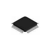
ispPAC-POWR1014-01T48I Lattice, ispPAC-POWR1014-01T48I Datasheet - Page 2

ispPAC-POWR1014-01T48I
Manufacturer Part Number
ispPAC-POWR1014-01T48I
Description
Supervisory Circuits Prec. Prog. Pwr Sppl y Seq. Mon. Trim I
Manufacturer
Lattice
Series
ispPAC®r
Datasheet
1.ISPPAC-POWR1014A-01TN48I.pdf
(52 pages)
Specifications of ispPAC-POWR1014-01T48I
Number Of Voltages Monitored
10
Output Type
Open Collector / Drain
Manual Reset
Not Resettable
Watchdog
No Watchdog
Power-up Reset Delay (typ)
500 ms
Supply Voltage (max)
3.96 V
Supply Voltage (min)
2.8 V
Supply Current (typ)
20 mA
Mounting Style
SMD/SMT
Package / Case
TQFP-48
Applications
General Purpose
Voltage - Input
-0.3 V ~ 5.9 V
Voltage - Supply
2.8 V ~ 3.96 V
Current - Supply
20mA
Operating Temperature
-40°C ~ 85°C
Mounting Type
*
Lead Free Status / Rohs Status
Lead free / RoHS Compliant
Available stocks
Company
Part Number
Manufacturer
Quantity
Price
Company:
Part Number:
ISPPAC-POWR1014-01T48I
Manufacturer:
Lattice Semiconductor Corporation
Quantity:
10 000
Part Number:
ISPPAC-POWR1014-01T48I
Manufacturer:
LATTICE
Quantity:
20 000
Lattice Semiconductor
MOSFET drivers. In high-voltage mode these outputs can provide up to 12V for driving the gates of n-channel
MOSFETs so that they can be used as high-side power switches controlling the supplies with a programmable
ramp rate for both ramp up and ramp down.
The ispPAC-POWR1014/A incorporates a 24-macrocell CPLD that can be used to implement complex state
machine sequencing for the control of multiple power supplies as well as combinatorial logic functions. The status
of all of the comparators on the analog input channels as well as the general purpose digital inputs are used as
inputs by the CPLD array, and all digital outputs may be controlled by the CPLD. Four independently programmable
timers can create delays and time-outs ranging from 32µs to 2 seconds. The CPLD is programmed using Logi-
Builder™, an easy-to-learn language integrated into the PAC-Designer
monitor the status of any of the analog input channel comparators or the digital inputs.
The on-chip 10-bit A/D converter is used to monitor the V
ispPAC-POWR1014A device.
The I
inputs, read back the status of each of the V
control the output pins (ispPAC-POWR1014A only). The JTAG interface can be used to read out all I
during manufacturing.
Figure 2-1. ispPAC-POWR1014/A Block Diagram
2
C bus/SMBus interface allows an external microcontroller to measure the voltages connected to the V
VMON10
VMON1
VMON2
VMON3
VMON4
VMON5
VMON6
VMON7
VMON8
VMON9
IN1
IN2
IN3
IN4
*ispPAC-POWR1014A only.
ADC*
JTAG LOGIC
MON
OSCILLATOR
comparator and PLD outputs, control logic signals IN2 to IN4 and
24 MACROCELLS
CONTROL LOGIC*
CLOCK
MEASUREMENT
53 INPUTS
CPLD
2-2
MON
TIMERS
voltage through the I
(4)
®
ispPAC-POWR1014/A Data Sheet
software. Control sequences are written to
INTERFACE
I
2
C
2
C bus or JTAG interface of the
HVOUT1
HVOUT2
OUT3/(SMBA*)
OUT4
OUT5
OUT6
OUT7
OUT8
OUT9
OUT10
OUT11
OUT12
OUT13
OUT14
2
C registers
MON


