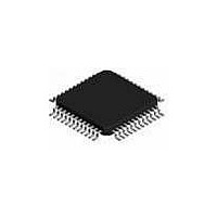
ispPAC-POWR1014-01T48I Lattice, ispPAC-POWR1014-01T48I Datasheet - Page 20

ispPAC-POWR1014-01T48I
Manufacturer Part Number
ispPAC-POWR1014-01T48I
Description
Supervisory Circuits Prec. Prog. Pwr Sppl y Seq. Mon. Trim I
Manufacturer
Lattice
Series
ispPAC®r
Datasheet
1.ISPPAC-POWR1014A-01TN48I.pdf
(52 pages)
Specifications of ispPAC-POWR1014-01T48I
Number Of Voltages Monitored
10
Output Type
Open Collector / Drain
Manual Reset
Not Resettable
Watchdog
No Watchdog
Power-up Reset Delay (typ)
500 ms
Supply Voltage (max)
3.96 V
Supply Voltage (min)
2.8 V
Supply Current (typ)
20 mA
Mounting Style
SMD/SMT
Package / Case
TQFP-48
Applications
General Purpose
Voltage - Input
-0.3 V ~ 5.9 V
Voltage - Supply
2.8 V ~ 3.96 V
Current - Supply
20mA
Operating Temperature
-40°C ~ 85°C
Mounting Type
*
Lead Free Status / Rohs Status
Lead free / RoHS Compliant
Available stocks
Company
Part Number
Manufacturer
Quantity
Price
Company:
Part Number:
ISPPAC-POWR1014-01T48I
Manufacturer:
Lattice Semiconductor Corporation
Quantity:
10 000
Part Number:
ISPPAC-POWR1014-01T48I
Manufacturer:
LATTICE
Quantity:
20 000
Lattice Semiconductor
PLD Block
Figure 2-10 shows the ispPAC-POWR1014/A PLD architecture, which is derived from the Lattice ispMACH
CPLD. The PLD architecture allows the flexibility in designing various state machines and control functions used for
power supply management. The AND array has 53 inputs and generates 123 product terms. These 123 product
terms are divided into three groups of 41 for each of the generic logic blocks, GLB1, GLB2, and GLB3. Each GLB
is made up of eight macrocells. In total, there are 24 macrocells in the ispPAC-POWR1014/A device. The output
signals of the ispPAC-POWR1014/A device are derived from GLBs as shown in Figure 2-10. GLB3 generates timer
control.
Figure 2-10. ispPAC-POWR1014/A PLD Architecture
Macrocell Architecture
The macrocell shown in Figure 2-11 is the heart of the PLD. The basic macrocell has five product terms that feed
the OR gate and the flip-flop. The flip-flop in each macrocell is independently configured. It can be programmed to
function as a D-Type or T-Type flip-flop. Combinatorial functions are realized by bypassing the flip-flop. The polarity
control and XOR gates provide additional flexibility for logic synthesis. The flip-flop’s clock is driven from the com-
mon PLD clock that is generated by dividing the 8 MHz master clock by 32. The macrocell also supports asynchro-
nous reset and preset functions, derived from either product terms, the global reset input, or the power-on reset
signal. The resources within the macrocells share routing and contain a product term allocation array. The product
term allocation array greatly expands the PLD’s ability to implement complex logical functions by allowing logic to
be shared between adjacent blocks and distributing the product terms to allow for wider decode functions. All the
digital inputs are registered by MCLK and the VMON comparator outputs are registered by the PLD Clock to syn-
chronize them to the PLD logic.
Global Reset
(Resetb pin)
AGOOD
IN[1:4]
VMON[1-10]
20
4
Timer0
Timer1
Timer2
Timer3
Register
Register
MCLK
Input
Input
Output
Feedback
Timer Clock
4
24
IRP
AND Array
53 Inputs
123 PT
18
PLD Clock
41
41
41
2-20
Generic Logic Block
Generic Logic Block
Generic Logic Block
8 Macrocell
8 Macrocell
8 Macrocell
GLB1
41 PT
GLB2
41 PT
GLB3
41 PT
ispPAC-POWR1014/A Data Sheet
HVOUT[1..2],
OUT[3..8]
OUT[9..14]
®
4000


