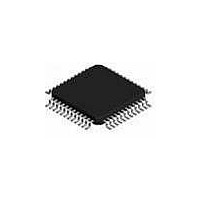
ispPAC-POWR1014-01T48I Lattice, ispPAC-POWR1014-01T48I Datasheet - Page 41

ispPAC-POWR1014-01T48I
Manufacturer Part Number
ispPAC-POWR1014-01T48I
Description
Supervisory Circuits Prec. Prog. Pwr Sppl y Seq. Mon. Trim I
Manufacturer
Lattice
Series
ispPAC®r
Datasheet
1.ISPPAC-POWR1014A-01TN48I.pdf
(52 pages)
Specifications of ispPAC-POWR1014-01T48I
Number Of Voltages Monitored
10
Output Type
Open Collector / Drain
Manual Reset
Not Resettable
Watchdog
No Watchdog
Power-up Reset Delay (typ)
500 ms
Supply Voltage (max)
3.96 V
Supply Voltage (min)
2.8 V
Supply Current (typ)
20 mA
Mounting Style
SMD/SMT
Package / Case
TQFP-48
Applications
General Purpose
Voltage - Input
-0.3 V ~ 5.9 V
Voltage - Supply
2.8 V ~ 3.96 V
Current - Supply
20mA
Operating Temperature
-40°C ~ 85°C
Mounting Type
*
Lead Free Status / Rohs Status
Lead free / RoHS Compliant
Available stocks
Company
Part Number
Manufacturer
Quantity
Price
Company:
Part Number:
ISPPAC-POWR1014-01T48I
Manufacturer:
Lattice Semiconductor Corporation
Quantity:
10 000
Part Number:
ISPPAC-POWR1014-01T48I
Manufacturer:
LATTICE
Quantity:
20 000
Lattice Semiconductor
PLD_VERIFY – This instruction is used to read the content of the selected PLD AND/ARCH array column. This
specific column is preselected by using PLD_ADDRESS_SHIFT instruction. This instruction also forces the outputs
into the OUTPUTS_HIGHZ.
DISCHARGE – This instruction is used to discharge the internal programming supply voltage after an erase or pro-
gramming cycle and prepares ispPAC-POWR1014/A for a read cycle. This instruction also forces the outputs into
the OUTPUTS_HIGHZ.
CFG_ADDRESS – This instruction is used to set the address of the CFG array for subsequent program or read
operations. This instruction also forces the outputs into the OUTPUTS_HIGHZ.
CFG_DATA_SHIFT – This instruction is used to shift data into the CFG register prior to programming or reading.
This instruction also forces the outputs into the OUTPUTS_HIGHZ.
CFG_ERASE – This instruction will bulk erase the CFG array. The action occurs at the second rising edge of TCK
in Run-Test-Idle JTAG state. The device must already be in programming mode (PROGRAM_ENABLE instruction).
This instruction also forces the outputs into the OUTPUTS_HIGHZ.
CFG_PROGRAM – This instruction programs the selected CFG array column. This specific column is preselected
by using CFG_ADDRESS instruction. The programming occurs at the second rising edge of the TCK in Run-Test-
Idle JTAG state. The device must already be in programming mode (PROGRAM_ENABLE instruction). This
instruction also forces the outputs into the OUTPUTS_HIGHZ.
CFG_VERIFY – This instruction is used to read the content of the selected CFG array column. This specific col-
umn is preselected by using CFG_ADDRESS instruction. This instruction also forces the outputs into the
OUTPUTS_HIGHZ.
BULK_ERASE – This instruction will bulk erase all E
POWR1014/A. The device must already be in programming mode (PROGRAM_ENABLE instruction). This instruc-
tion also forces the outputs into the OUTPUTS_HIGHZ.
OUTPUTS_HIGHZ – This instruction turns off all of the open-drain output transistors. Pins that are programmed as
FET drivers will be placed in the active low state. This instruction is effective after Update-Instruction-Register
JTAG state.
PROGRAM_ENABLE – This instruction enables the programming mode of the ispPAC-POWR1014/A. This
instruction also forces the outputs into the OUTPUTS_HIGHZ.
IDCODE – This instruction connects the output of the Identification Code Data Shift (IDCODE) Register to TDO
(Figure 2-33), to support reading out the identification code.
Figure 2-33. IDCODE Register
PROGRAM_DISABLE – This instruction disables the programming mode of the ispPAC-POWR1014/A. The Test-
Logic-Reset JTAG state can also be used to cancel the programming mode of the ispPAC-POWR1014/A.
UES_READ – This instruction both reads the E
between the TDI and TDO pins (as shown in Figure 2-30), to support programming or reading of the user electronic
signature bits.
Bit
31
Bit
30
Bit
29
Bit
28
Bit
27
2
CMOS bits into the UES register and places the UES register
2-41
2
CMOS bits (CFG, PLD, UES, and ESF) in the ispPAC-
Bit
4
ispPAC-POWR1014/A Data Sheet
Bit
3
Bit
2
Bit
1
Bit
0
TDO


