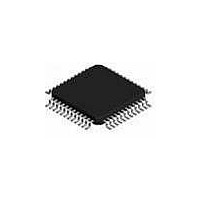
ispPAC-POWR1014-01T48I Lattice, ispPAC-POWR1014-01T48I Datasheet - Page 4

ispPAC-POWR1014-01T48I
Manufacturer Part Number
ispPAC-POWR1014-01T48I
Description
Supervisory Circuits Prec. Prog. Pwr Sppl y Seq. Mon. Trim I
Manufacturer
Lattice
Series
ispPAC®r
Datasheet
1.ISPPAC-POWR1014A-01TN48I.pdf
(52 pages)
Specifications of ispPAC-POWR1014-01T48I
Number Of Voltages Monitored
10
Output Type
Open Collector / Drain
Manual Reset
Not Resettable
Watchdog
No Watchdog
Power-up Reset Delay (typ)
500 ms
Supply Voltage (max)
3.96 V
Supply Voltage (min)
2.8 V
Supply Current (typ)
20 mA
Mounting Style
SMD/SMT
Package / Case
TQFP-48
Applications
General Purpose
Voltage - Input
-0.3 V ~ 5.9 V
Voltage - Supply
2.8 V ~ 3.96 V
Current - Supply
20mA
Operating Temperature
-40°C ~ 85°C
Mounting Type
*
Lead Free Status / Rohs Status
Lead free / RoHS Compliant
Available stocks
Company
Part Number
Manufacturer
Quantity
Price
Company:
Part Number:
ISPPAC-POWR1014-01T48I
Manufacturer:
Lattice Semiconductor Corporation
Quantity:
10 000
Part Number:
ISPPAC-POWR1014-01T48I
Manufacturer:
LATTICE
Quantity:
20 000
Pin Descriptions (Cont.)
Lattice Semiconductor
Number
1. [IN1...IN4] are inputs to the PLD. The thresholds for these pins are referenced by the voltage on VCCINP. Unused INx inputs should be tied
2. IN1 pin can also be controlled through JTAG interface.
3. [IN2..IN4] can also be controlled through I
4. GNDA and GNDD pins must be connected together on the circuit board.
5. VCCD and VCCA pins must be connected together on the circuit board.
6. Open-drain outputs require an external pull-up resistor to a supply.
7. The RESETb pin should only be used for cascading two or more ispPAC-POWR1014/A devices.
8. These pins should be connected to GNDD (ispPAC-POWR1014 only).
9. The VCCPROG pin MUST be left floating when V
10. SCL should be tied high and SDA is don’t care when I
42
43
21
22
16
18
17
19
39
38
to GNDD.
PLDCLK
MCLK
TDO
TCK
TMS
TDI
ATDI
TDISEL
SCL
SDA
9, 11
Name
9, 11
Digital Output
Digital I/O
Digital Output
Digital Input
Digital Input
Digital Input
Digital Input
Digital Input
Digital Input
Digital I/O
Pin Type
2
C/SMBus interface (ispPAC-POWR1014A only).
CCD
0V to 3.96V
0V to 3.96V
0V to 5.5V
0V to 5.5V
0V to 5.5V
0V to 5.5V
0V to 5.5V
0V to 5.5V
0V to 5.5V
0V to 5.5V
2
and V
C registers are accessed through the JTAG interface (ispPAC-POWR1014A only).
Voltage Range
CCA
are powered.
2-4
250kHz PLD Clock Output (Tristate), CMOS
Output
Pin internally pulled up.
8MHz Clock I/O (Tristate), CMOS Drive.
Pin internally pulled up.
JTAG Test Data Out
JTAG Test Clock Input
JTAG Test Mode Select
Pin internally pulled up.
JTAG Test Data In, TDISEL pin = 1.Pin internally
pulled up.
JTAG Test Data In (Alternate), TDISEL Pin =
0.Pin internally pulled up.
Select TDI/ATDI Input
Pin internally pulled up.
I
Only)
I
(ispPAC-POWR1014A Only)
2
2
C Serial Clock Input (ispPAC-POWR1014A
C Serial Data, Bi-directional Pin, Open Drain
ispPAC-POWR1014/A Data Sheet
Description


