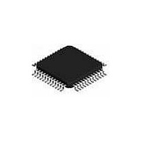
ispPAC-POWR1014-01T48I Lattice, ispPAC-POWR1014-01T48I Datasheet - Page 44

ispPAC-POWR1014-01T48I
Manufacturer Part Number
ispPAC-POWR1014-01T48I
Description
Supervisory Circuits Prec. Prog. Pwr Sppl y Seq. Mon. Trim I
Manufacturer
Lattice
Series
ispPAC®r
Datasheet
1.ISPPAC-POWR1014A-01TN48I.pdf
(52 pages)
Specifications of ispPAC-POWR1014-01T48I
Number Of Voltages Monitored
10
Output Type
Open Collector / Drain
Manual Reset
Not Resettable
Watchdog
No Watchdog
Power-up Reset Delay (typ)
500 ms
Supply Voltage (max)
3.96 V
Supply Voltage (min)
2.8 V
Supply Current (typ)
20 mA
Mounting Style
SMD/SMT
Package / Case
TQFP-48
Applications
General Purpose
Voltage - Input
-0.3 V ~ 5.9 V
Voltage - Supply
2.8 V ~ 3.96 V
Current - Supply
20mA
Operating Temperature
-40°C ~ 85°C
Mounting Type
*
Lead Free Status / Rohs Status
Lead free / RoHS Compliant
Available stocks
Company
Part Number
Manufacturer
Quantity
Price
Company:
Part Number:
ISPPAC-POWR1014-01T48I
Manufacturer:
Lattice Semiconductor Corporation
Quantity:
10 000
Part Number:
ISPPAC-POWR1014-01T48I
Manufacturer:
LATTICE
Quantity:
20 000
Lattice Semiconductor
Figure 2-36. VMON Status Registers
ADC Interface Registers
Byte 6, Byte 5: These bytes contain 12-bit ADC measured values.
Figure 2-37. ADC Interface Registers, Bytes 6 and 5
Byte 4: The I2C_Data_Register write operation action is determined by bit 6 of the I2C_Control_Register. When bit
6 of the I2C_Control_Register is set to 1, this byte selects the VMON input for routing to the ADC (4-bit ADC input
mux) and sets/clears the ADC attenuate mode. When the bit 6 of the I2C_Control_register is reset to 0, the con-
tents of the Byte 4 are ignored. During I2C_Data_Register read operation with bit 6 reset to 0 in the
I2C_Control_Register, byte 4 returns the 4-bit input mux setting and the attenuate bit setting. Refer to Tables 2-8
and 2-9 for the mux select and the attenuate bits decode value.
Figure 2-38. ADC Interface Registers, Byte 4
Digital Input Status and Input Value Register
Byte 3: I2C_Control_Register bits 5 and 4 control reading into and writing from Byte 3 of the I2C_Data_Register.
When bits 5 and 4 are set to 10b, the contents of Byte 3 are written into the input register bits during the
I2C_Data_Register write operation.
Figure 2-39. INPUT_VALUE Registers, Byte 3
Byte 3 – INPUT_VALUE (Write Operation) – When I2C_Control_Register bit 5 =1, bit 4=0, I
(23)
X
Byte 5 – ADC_Value_High (Read Only), I
Byte 4 – ADC_MUX (Read/ Write), I
Byte 6 – ADC_Value_Low (Read Only), I
Byte 9 – VMON_STATUS0 (Read Only, Most Significant), I
Byte 8 – VMON_STATUS1 (Read Only), I
Byte 7 – VMON_STATUS2 (Read Only), I
VMON1A
VMON5A
VMON9A
SEL0
(47)
(39)
(71)
(63)
(55)
D4
(31)
X
(22)
I2
VMON5B
VMON1B
VMON9B
SEL1
(62)
(70)
(38)
(54)
(46)
(30)
D5
1
(21)
I3
VMON10A
VMON2A
VMON6A
SEL2
(37)
(69)
(29)
(61)
(53)
(45)
D6
1
(20)
I4
2
VMON10B
VMON2B
C Address = 0x09
VMON6B
SEL3
(36)
(68)
(44)
(28)
(52)
(60)
D7
1
(19)
2
2
1
2
2
C Address = 0x07
C Address = 0x08
C Address = 0x01
C Address = 0x02
2-44
VMON3A
VMON7A
ATTEN
(43)
(35)
(67)
(59)
(27)
D0
D8
(51)
1
(18)
1
VMON3B
VMON7B
2
C Address = 0x00
(26)
(66)
(58)
(50)
(42)
(34)
D1
D9
X
1
(17)
ispPAC-POWR1014/A Data Sheet
1
VMON4A
VMON8A
(65)
(25)
(57)
(49)
D10
(33)
(41)
D2
X
1
(16)
1
VMON4B
VMON8B
2
C Address = 0x11
(64)
D11
(32)
(24)
(56)
(48)
(40)
D3
X
1


