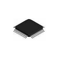
ispPAC-POWR1014-01T48I Lattice, ispPAC-POWR1014-01T48I Datasheet - Page 40

ispPAC-POWR1014-01T48I
Manufacturer Part Number
ispPAC-POWR1014-01T48I
Description
Supervisory Circuits Prec. Prog. Pwr Sppl y Seq. Mon. Trim I
Manufacturer
Lattice
Series
ispPAC®r
Datasheet
1.ISPPAC-POWR1014A-01TN48I.pdf
(52 pages)
Specifications of ispPAC-POWR1014-01T48I
Number Of Voltages Monitored
10
Output Type
Open Collector / Drain
Manual Reset
Not Resettable
Watchdog
No Watchdog
Power-up Reset Delay (typ)
500 ms
Supply Voltage (max)
3.96 V
Supply Voltage (min)
2.8 V
Supply Current (typ)
20 mA
Mounting Style
SMD/SMT
Package / Case
TQFP-48
Applications
General Purpose
Voltage - Input
-0.3 V ~ 5.9 V
Voltage - Supply
2.8 V ~ 3.96 V
Current - Supply
20mA
Operating Temperature
-40°C ~ 85°C
Mounting Type
*
Lead Free Status / Rohs Status
Lead free / RoHS Compliant
Available stocks
Company
Part Number
Manufacturer
Quantity
Price
Company:
Part Number:
ISPPAC-POWR1014-01T48I
Manufacturer:
Lattice Semiconductor Corporation
Quantity:
10 000
Part Number:
ISPPAC-POWR1014-01T48I
Manufacturer:
LATTICE
Quantity:
20 000
Lattice Semiconductor
The EXTEST (external test) instruction is required and would normally place the device into an external boundary
test mode while also enabling the boundary scan register to be connected between TDI and TDO. Again, since the
ispPAC-POWR1014/A has no boundary scan logic, the device is put in the BYPASS mode to ensure specification
compatibility. The bit code of this instruction is defined by the 1149.1 standard to be all zeros (00000000).
The optional IDCODE (identification code) instruction is incorporated in the ispPAC-POWR1014/A and leaves it in
its functional mode when executed. It selects the Device Identification Register to be connected between TDI and
TDO. The Identification Register is a 32-bit shift register containing information regarding the IC manufacturer,
device type and version code (Figure 2-32). Access to the Identification Register is immediately available, via a
TAP data scan operation, after power-up of the device, or by issuing a Test-Logic-Reset instruction. The bit code for
this instruction is defined by Lattice as shown in Table 2-11.
Figure 2-32. ispPAC-POWR1014/A ID Code
ispPAC-POWR1014/A Specific Instructions
There are 25 unique instructions specified by Lattice for the ispPAC-POWR1014/A. These instructions are primarily
used to interface to the various user registers and the E
used to control or monitor other features of the device. A brief description of each unique instruction is provided in
detail below, and the bit codes are found in Table 2-11.
PLD_ADDRESS_SHIFT – This instruction is used to set the address of the PLD AND/ARCH arrays for subsequent
program or read operations. This instruction also forces the outputs into the OUTPUTS_HIGHZ.
PLD_DATA_SHIFT – This instruction is used to shift PLD data into the register prior to programming or reading.
This instruction also forces the outputs into the OUTPUTS_HIGHZ.
PLD_INIT_ADDR_FOR_PROG_INCR – This instruction prepares the PLD address register for subsequent
PLD_PROG_INCR or PLD_VERIFY_INCR instructions.
PLD_PROG_INCR – This instruction programs the PLD data register for the current address and increments the
address register for the next set of data.
PLD_PROGRAM – This instruction programs the selected PLD AND/ARCH array column. The specific column is
preselected by using PLD_ADDRESS_SHIFT instruction. The programming occurs at the second rising edge of
the TCK in Run-Test-Idle JTAG state. The device must already be in programming mode (PROGRAM_ENABLE
instruction). This instruction also forces the outputs into the OUTPUTS_HIGHZ.
PROGRAM_SECURITY – This instruction is used to program the electronic security fuse (ESF) bit. Programming
the ESF bit protects proprietary designs from being read out. The programming occurs at the second rising edge of
the TCK in Run-Test-Idle JTAG state. The device must already be in programming mode (PROGRAM_ENABLE
instruction). This instruction also forces the outputs into the OUTPUTS_HIGHZ.
00145h = ispPAC-POWR1014A-1
10145h = ispPAC-POWR1014-1
20145h = ispPAC-POWR1014A-2
30145h = ispPAC-POWR1014-2
0001 0000 0001 0100 0101 / 0000 0100 001 / 1
0000 0000 0001 0100 0101 / 0000 0100 001 / 1
0011 0000 0001 0100 0101 / 0000 0100 001 / 1
0010 0000 0001 0100 0101 / 0000 0100 001 / 1
MSB
Part Number
(20 bits)
Lattice Semiconductor
JEDEC Manufacturer
Identity Code for
(11 bits)
2-40
2
CMOS non-volatile memory. Additional instructions are
per 1149.1-1990
Constant 1
(1 bit)
LSB
ispPAC-POWR1014/A Data Sheet
(ispPAC-POWR1014-1)
(ispPAC-POWR1014A-1)
(ispPAC-POWR1014-2)
(ispPAC-POWR1014A-2)


