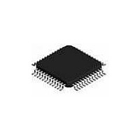
ispPAC-POWR1014-01T48I Lattice, ispPAC-POWR1014-01T48I Datasheet - Page 24

ispPAC-POWR1014-01T48I
Manufacturer Part Number
ispPAC-POWR1014-01T48I
Description
Supervisory Circuits Prec. Prog. Pwr Sppl y Seq. Mon. Trim I
Manufacturer
Lattice
Series
ispPAC®r
Datasheet
1.ISPPAC-POWR1014A-01TN48I.pdf
(52 pages)
Specifications of ispPAC-POWR1014-01T48I
Number Of Voltages Monitored
10
Output Type
Open Collector / Drain
Manual Reset
Not Resettable
Watchdog
No Watchdog
Power-up Reset Delay (typ)
500 ms
Supply Voltage (max)
3.96 V
Supply Voltage (min)
2.8 V
Supply Current (typ)
20 mA
Mounting Style
SMD/SMT
Package / Case
TQFP-48
Applications
General Purpose
Voltage - Input
-0.3 V ~ 5.9 V
Voltage - Supply
2.8 V ~ 3.96 V
Current - Supply
20mA
Operating Temperature
-40°C ~ 85°C
Mounting Type
*
Lead Free Status / Rohs Status
Lead free / RoHS Compliant
Available stocks
Company
Part Number
Manufacturer
Quantity
Price
Company:
Part Number:
ISPPAC-POWR1014-01T48I
Manufacturer:
Lattice Semiconductor Corporation
Quantity:
10 000
Part Number:
ISPPAC-POWR1014-01T48I
Manufacturer:
LATTICE
Quantity:
20 000
Lattice Semiconductor
CAUTION: Activating the RESETb signal or issuing a RESET command through I2C or JTAG during the ispPAC-
POWR1014/A device operation, results in the device aborting all operations and returning to the power-on reset
state. The status of the power supplies which are being enabled by the ispPAC-POWR1014/A will be determined by
the state of the outputs shown above.
I
I
devices on a circuit board. The ispPAC-POWR1014A supports a 7-bit addressing of the I
col, as well as SMBTimeout and SMBAlert features of the SMBus, enabling it to easily integrated into many types
of modern power management systems. Figure 2-15 shows a typical I
PAC-POWR1014As are slaved to a supervisory microcontroller. SDA is used to carry data signals, while SCL pro-
vides a synchronous clock signal. The SMBAlert line is only present in SMBus systems. The 7-bit I
the POWR1014A is fully programmable through the JTAG port.
Figure 2-15. ispPAC-POWR1014A in I
In both the I
ter device generates the SCL clock signal and coordinates all data transfers to and from a number of slave devices.
The ispPAC-POWR1014A is configured as a slave device, and cannot independently coordinate data transfers.
Each slave device on a given I
addressing portion of the standard. Any 7-bit address can be assigned to the ispPAC-POWR1014A device by pro-
gramming through JTAG. When selecting a device address, one should note that several addresses are reserved
by the I
compatibility. Table 2-6 lists these reserved addresses.
2
2
C and SMBus are low-speed serial interface protocols designed to enable communications among a number of
C/SMBUS Interface (ispPAC-POWR1014A Only)
2
C and/or SMBus standards, and should not be assigned to ispPAC-POWR1014A devices to assure bus
SDA
V+
2
C and SMBus protocols, the bus is controlled by a single MASTER device at any given time. This mas-
MICROPROCESSOR
(I
2
SCL
C MASTER)
INTERRUPT
2
C bus is assigned a unique address. The ispPAC-POWR1014A implements the 7-bit
SDA/SMDAT (DATA)
SCL/SMCLK (CLOCK)
SMBALERT
2
C/SMBUS System
SDA
POWR1014A
(I
2-24
2
C SLAVE)
SCL
OUT5/
SMBA
2
ispPAC-POWR1014/A Data Sheet
C configuration, in which one or more isp-
SDA
POWR1014A
(I
2
C SLAVE)
SCL
2
C communications proto-
OUT5/
SMBA
To Other
2
Devices
C address of
I
2
C


