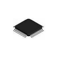
ispPAC-POWR1014-01T48I Lattice, ispPAC-POWR1014-01T48I Datasheet - Page 22

ispPAC-POWR1014-01T48I
Manufacturer Part Number
ispPAC-POWR1014-01T48I
Description
Supervisory Circuits Prec. Prog. Pwr Sppl y Seq. Mon. Trim I
Manufacturer
Lattice
Series
ispPAC®r
Datasheet
1.ISPPAC-POWR1014A-01TN48I.pdf
(52 pages)
Specifications of ispPAC-POWR1014-01T48I
Number Of Voltages Monitored
10
Output Type
Open Collector / Drain
Manual Reset
Not Resettable
Watchdog
No Watchdog
Power-up Reset Delay (typ)
500 ms
Supply Voltage (max)
3.96 V
Supply Voltage (min)
2.8 V
Supply Current (typ)
20 mA
Mounting Style
SMD/SMT
Package / Case
TQFP-48
Applications
General Purpose
Voltage - Input
-0.3 V ~ 5.9 V
Voltage - Supply
2.8 V ~ 3.96 V
Current - Supply
20mA
Operating Temperature
-40°C ~ 85°C
Mounting Type
*
Lead Free Status / Rohs Status
Lead free / RoHS Compliant
Available stocks
Company
Part Number
Manufacturer
Quantity
Price
Company:
Part Number:
ISPPAC-POWR1014-01T48I
Manufacturer:
Lattice Semiconductor Corporation
Quantity:
10 000
Part Number:
ISPPAC-POWR1014-01T48I
Manufacturer:
LATTICE
Quantity:
20 000
Lattice Semiconductor
cuits and ADC. The ispPAC-POWR1014/A can be programmed to operate in three modes: Master mode, Stand-
alone mode and Slave mode. Table 2-5 summarizes the operating modes of ispPAC-POWR1014/A.
Table 2-5. ispPAC-POWR1014/A Operating Modes
A divide-by-32 prescaler divides the internal 8MHz oscillator (or external clock, if selected) down to 250kHz for the
PLD clock and for the programmable timers. This PLD clock may be made available on the PLDCLK pin by closing
SW2. Each of the four timers provides independent timeout intervals ranging from 32µs to 1.96 seconds in 128
steps.
Digital Outputs
The ispPAC-POWR1014/A provides 14 digital outputs, HVOUT[1:2] and OUT[3:14]. Outputs OUT[3:14] are perma-
nently configured as open drain to provide a high degree of flexibility when interfacing to logic signals, LEDs, opto-
couplers, and power supply control inputs. The HVOUT[1:2] pins can be configured as either high voltage FET driv-
ers or open drain outputs. Each of these outputs may be controlled either from the PLD or from the I
PAC-POWR1014A only). The determination whether a given output is under PLD or I
pin-by-pin basis (see Figure 2-13). For further details on controlling the outputs through I
SMBUS Interface and Accessing I
Figure 2-13. Digital Output Pin Configuration
High-Voltage Outputs
In addition to being usable as digital open-drain outputs, the ispPAC-POWR1014/A’s HVOUT1-HVOUT2 output
pins can be programmed to operate as high-voltage FET drivers. Figure 2-14 shows the details of the HVOUT gate
drivers. Each of these outputs may be controlled from the PLD, or with the ispPAC-POWR1014A, from the I
isters (see Figure 2-14). For further details on controlling the outputs through I
face, and Accessing I
Operating Mode
Standalone
Master
Slave
Timer
Closed
Closed
Open
SW0
2
C Registers Through JTAG sections of this data sheet.
Closed
Closed
Open
SW1
2
C Registers Through JTAG sections of this data sheet.
Digital Control from I
When only one ispPAC-POWR1014/A is used.
When more than one ispPAC-POWR1014/A is
used on a board, one of them should be configured
to operate in this mode.
When more than one ispPAC-POWR1014/As is
used on a board. Other than the master, the rest of
the ispPAC-POWR1014/As should be programmed
as slaves.
(ispPAC-POWR1014A only)
Digital Control
from PLD
Condition
2-22
2
C Register
ispPAC-POWR1014/A Data Sheet
OUTx
Pin
2
C, please see the I
MCLK pin tristated
MCLK pin outputs 8MHz clock
MCLK pin is input
2
C control may be made on a
2
C, please see the I
Comments
2
C/SMBUS Inter-
2
C register (isp-
2
C reg-
2
C/


