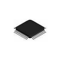
ispPAC-POWR1014-01T48I Lattice, ispPAC-POWR1014-01T48I Datasheet - Page 3

ispPAC-POWR1014-01T48I
Manufacturer Part Number
ispPAC-POWR1014-01T48I
Description
Supervisory Circuits Prec. Prog. Pwr Sppl y Seq. Mon. Trim I
Manufacturer
Lattice
Series
ispPAC®r
Datasheet
1.ISPPAC-POWR1014A-01TN48I.pdf
(52 pages)
Specifications of ispPAC-POWR1014-01T48I
Number Of Voltages Monitored
10
Output Type
Open Collector / Drain
Manual Reset
Not Resettable
Watchdog
No Watchdog
Power-up Reset Delay (typ)
500 ms
Supply Voltage (max)
3.96 V
Supply Voltage (min)
2.8 V
Supply Current (typ)
20 mA
Mounting Style
SMD/SMT
Package / Case
TQFP-48
Applications
General Purpose
Voltage - Input
-0.3 V ~ 5.9 V
Voltage - Supply
2.8 V ~ 3.96 V
Current - Supply
20mA
Operating Temperature
-40°C ~ 85°C
Mounting Type
*
Lead Free Status / Rohs Status
Lead free / RoHS Compliant
Available stocks
Company
Part Number
Manufacturer
Quantity
Price
Company:
Part Number:
ISPPAC-POWR1014-01T48I
Manufacturer:
Lattice Semiconductor Corporation
Quantity:
10 000
Part Number:
ISPPAC-POWR1014-01T48I
Manufacturer:
LATTICE
Quantity:
20 000
Pin Descriptions
Lattice Semiconductor
Number
41, 23 VCCD
7, 31
44
46
47
48
26
27
28
32
33
34
35
36
37
30
29
45
20
24
15
14
13
12
11
10
40
25
9
8
6
5
4
3
2
1
IN1
IN2
IN3
IN4
VMON1
VMON2
VMON3
VMON4
VMON5
VMON6
VMON7
VMON8
VMON9
VMON10
GNDD
GNDA
VCCA
VCCINP
VCCJ
VCCPROG
HVOUT1
HVOUT2
SMBA_OUT3
OUT4
OUT5
OUT6
OUT7
OUT8
OUT9
OUT10
OUT11
OUT12
OUT13
OUT14
RESETb
Name
5
4
5
4
7
9
Digital Input
Digital Input
Digital Input
Digital Input
Analog Input
Analog Input
Analog Input
Analog Input
Analog Input
Analog Input
Analog Input
Analog Input
Analog Input
Analog Input
Ground
Ground
Power
Power
Power
Power
Power
Open Drain Output
Current Source/Sink
Open Drain Output
Current Source/Sink
Open Drain Output
Open Drain Output
Open Drain Output
Open Drain Output
Open Drain Output
Open Drain Output
Open Drain Output
Open Drain Output
Open Drain Output
Open Drain Output
Open Drain Output
Open Drain Output
Digital I/O
Pin Type
6
6
6
6
6
6
6
6
6
6
6
6
6
6
VCCINP
VCCINP
VCCINP
VCCINP
-0.3V to 5.87V
-0.3V to 5.87V
-0.3V to 5.87V
-0.3V to 5.87V
-0.3V to 5.87V
-0.3V to 5.87V
-0.3V to 5.87V
-0.3V to 5.87V
-0.3V to 5.87V
-0.3V to 5.87V
Ground
Ground
2.8V to 3.96V
2.8V to 3.96V
2.25V to 5.5V
2.25V to 3.6V
3.0V to 3.6V
0V to 13V
12.5µA to 100µA Source
100µA to 3000µA Sink
0V to 13V
12.5µA to 100µA Source
100µA to 3000µA Sink
0V to 5.5V
0V to 5.5V
0V to 5.5V
0V to 5.5V
0V to 5.5V
0V to 5.5V
0V to 5.5V
0V to 5.5V
0V to 5.5V
0V to 5.5V
0V to 5.5V
0V to 5.5V
0V to 3.96V
Voltage Range
1, 2
1, 3
1, 3
1, 3
2-3
PLD Logic Input 1 Registered by MCLK
PLD Logic Input 2 Registered by MCLK
PLD Logic Input 3 Registered by MCLK
PLD Logic Input 4 Registered by MCLK
Voltage Monitor 1 Input
Voltage Monitor 2 Input
Voltage Monitor 3 Input
Voltage Monitor 4 Input
Voltage Monitor 5 Input
Voltage Monitor 6 Input
Voltage Monitor 7 Input
Voltage Monitor 8 Input
Voltage Monitor 9 Input
Voltage Monitor 10 Input
Digital Ground
Analog Ground
Core VCC, Main Power Supply
Analog Power Supply
VCC for IN[1:4] Inputs
VCC for JTAG Logic Interface Pins
VCC for E
is NOT Powered by V
must be floating.
Open-Drain Output 1
High-voltage FET Gate Driver 1
Open-Drain Output 2
High-voltage FET Gate Driver 2
Open-Drain Output 3, (SMBUS Alert Active Low,
ispPAC-POWR1014A only).
Open-Drain Output 4
Open-Drain Output 5
Open-Drain Output 6
Open-Drain Output 7
Open-Drain Output 8
Open-Drain Output 9
Open-Drain Output 10
Open-Drain Output 11
Open-Drain Output 12
Open-Drain Output 13
Open-Drain Output 14
Device Reset (Active Low)
Pin internally pulled up.
ispPAC-POWR1014/A Data Sheet
2
Programming Only when the Device
Description
CCD
and V
CCA
, otherwise,


