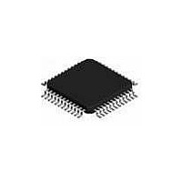
ispPAC-POWR1014-01T48I Lattice, ispPAC-POWR1014-01T48I Datasheet - Page 23

ispPAC-POWR1014-01T48I
Manufacturer Part Number
ispPAC-POWR1014-01T48I
Description
Supervisory Circuits Prec. Prog. Pwr Sppl y Seq. Mon. Trim I
Manufacturer
Lattice
Series
ispPAC®r
Datasheet
1.ISPPAC-POWR1014A-01TN48I.pdf
(52 pages)
Specifications of ispPAC-POWR1014-01T48I
Number Of Voltages Monitored
10
Output Type
Open Collector / Drain
Manual Reset
Not Resettable
Watchdog
No Watchdog
Power-up Reset Delay (typ)
500 ms
Supply Voltage (max)
3.96 V
Supply Voltage (min)
2.8 V
Supply Current (typ)
20 mA
Mounting Style
SMD/SMT
Package / Case
TQFP-48
Applications
General Purpose
Voltage - Input
-0.3 V ~ 5.9 V
Voltage - Supply
2.8 V ~ 3.96 V
Current - Supply
20mA
Operating Temperature
-40°C ~ 85°C
Mounting Type
*
Lead Free Status / Rohs Status
Lead free / RoHS Compliant
Available stocks
Company
Part Number
Manufacturer
Quantity
Price
Company:
Part Number:
ISPPAC-POWR1014-01T48I
Manufacturer:
Lattice Semiconductor Corporation
Quantity:
10 000
Part Number:
ISPPAC-POWR1014-01T48I
Manufacturer:
LATTICE
Quantity:
20 000
Lattice Semiconductor
Figure 2-14. Basic Function Diagram for an Output in High Voltage MOSFET Gate Driver Mode
Figure 2-14 shows the HVOUT circuitry when programmed as a FET driver. In this mode the output either sources
current from a charge pump or sinks current. The maximum voltage that the output level at the pin will rise to is also
programmable between 6V and 12V
threshold of the FET being driven and the power supply voltage being switched. The maximum voltage level needs
to be sufficient to bias the gate-to-source threshold on and also accommodate the load voltage at the FET’s
source, since the source pin of the FET to provide a wide range of ramp rates is tied to the supply of the target
board. When the HVOUT pin is sourcing current, charging a FET gate, the source current is programmable
between 12.5µA and 100µA. When the driver is turned to the off state, the driver will sink current to ground, and
this sink current is also programmable between 3000µA and 100µA to control the turn-off rate.
Programmable Output Voltage Levels for HVOUT1- HVOUT2
There are four
that the pin is capable of driving to can be programmed from 6V to 12V
1. -01 performance grade devices provide three selectable output voltage settings from 6V to 10V in 2V steps. The -02 performance grade
RESETb Signal, RESET Command via JTAG or I
Activating the RESETb signal (Logic 0 applied to the RESETb pin) or issuing a reset instruction via JTAG, or with
the ispPAC-POWR1014A, I
been configured in the PINS window:
At the conclusion of the RESET event, these outputs will go to the states defined by the PINS window, and if a
sequence has been programmed into the device, it will be re-started at the first step. The analog calibration will be
re-done and consequently, the VMONs, and ADCs will not be operational until 500 microseconds (max.) after the
conclusion of the RESET event.
devices also support the 12V output voltage setting.
• OUT3-14 will go high-impedance.
• HVOUT pins programmed for open drain operation will go high-impedance.
• HVOUT pins programmed for FET driver mode operation will pull down.
1
selectable steps for the output voltage of the FET drivers when in FET driver mode. The voltage
Digital Control from I
(ispPAC-POWR1014A Only)
Digital Control
2
C will force the outputs to the following states independent of how these outputs have
from PLD
1. -01 performance grade devices provide three selectable output voltage settings
Charge Pump
12V output voltage setting.
from 6V to 10V in 2V steps. The -02 performance grade devices also support the
(6 to 12V
1
. The maximum voltage levels that are required depend on the gate-to-source
1
)
2
C Register
+
-
(100 to 500 µA)
+Fast Turn-off
(3000µA)
I
SINK
2-23
2
(12.5 to 100 µA)
C
I
SOURCE
1
ispPAC-POWR1014/A Data Sheet
HVOUTx
in 2V steps.
Pin
Supply
Input
Load


