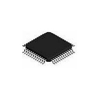
ispPAC-POWR1014-01T48I Lattice, ispPAC-POWR1014-01T48I Datasheet - Page 25

ispPAC-POWR1014-01T48I
Manufacturer Part Number
ispPAC-POWR1014-01T48I
Description
Supervisory Circuits Prec. Prog. Pwr Sppl y Seq. Mon. Trim I
Manufacturer
Lattice
Series
ispPAC®r
Datasheet
1.ISPPAC-POWR1014A-01TN48I.pdf
(52 pages)
Specifications of ispPAC-POWR1014-01T48I
Number Of Voltages Monitored
10
Output Type
Open Collector / Drain
Manual Reset
Not Resettable
Watchdog
No Watchdog
Power-up Reset Delay (typ)
500 ms
Supply Voltage (max)
3.96 V
Supply Voltage (min)
2.8 V
Supply Current (typ)
20 mA
Mounting Style
SMD/SMT
Package / Case
TQFP-48
Applications
General Purpose
Voltage - Input
-0.3 V ~ 5.9 V
Voltage - Supply
2.8 V ~ 3.96 V
Current - Supply
20mA
Operating Temperature
-40°C ~ 85°C
Mounting Type
*
Lead Free Status / Rohs Status
Lead free / RoHS Compliant
Available stocks
Company
Part Number
Manufacturer
Quantity
Price
Company:
Part Number:
ISPPAC-POWR1014-01T48I
Manufacturer:
Lattice Semiconductor Corporation
Quantity:
10 000
Part Number:
ISPPAC-POWR1014-01T48I
Manufacturer:
LATTICE
Quantity:
20 000
Lattice Semiconductor
Table 2-6. I
The ispPAC-POWR1014A’s I
write transaction (Figure 2-16) consists of the following operations:
To start the transaction, the master device holds the SCL line high while pulling SDA low. Address and data bits are
then transferred on each successive SCL pulse, in three consecutive byte frames of 9 SCL pulses. Address and
data are transferred on the first 8 SCL clocks in each frame, while an acknowledge signal is asserted by the slave
device on the 9th clock in each frame. Both data and addresses are transferred in a most-significant-bit-first format.
The first frame contains the 7-bit device address, with bit 8 held low to indicate a write operation. The second frame
contains the register address to which data will be written, and the final frame contains the actual data to be writ-
ten. Note that the SDA signal is only allowed to change when the SCL is low, as raising SDA when SCL is high sig-
nals the end of the transaction.
Figure 2-16. I
Reading a data byte from the ispPAC-POWR1014A requires two separate bus transactions (Figure 2-17). The first
transaction writes the register address from which a data byte is to be read. Note that since no data is being written
to the device, the transaction is concluded after the second byte frame. The second transaction performs the actual
read. The first frame contains the 7-bit device address with the R/W bit held High. In the second frame the ispPAC-
POWR1014A asserts data out on the bus in response to the SCL signal. Note that the acknowledge signal in the
second frame is asserted by the master device and not the ispPAC-POWR1014A.
1. Start the bus transaction
2. Transmit the device address (7 bits) along with a low write bit
3. Transmit the address of the register to be written to (8 bits)
4. Transmit the data to be written (8 bits)
5. Stop the bus transaction
SDA
SCL
2
C/SMBus Reserved Slave Device Addresses
START
0000 000
0000 000
0000 001
0000 010
0000 011
0000 1xx
0001 000
0001 100
0101 000
0110 111
1100 001
1111 0xx
1111 1xx
Address
2
C Write Operation
A6
1
A5
2
A4
DEVICE ADDRESS (7 BITS)
3
A3
4
R/W bit
2
C/SMBus interface allows data to be both written to and read from the device. A data
A2
5
0
1
x
x
x
x
x
x
x
x
x
x
x
A1
6
A0
7
R/W
8
General Call Address
Start Byte
CBUS Address
Reserved
Reserved
HS-mode master code
NA
NA
NA
NA
NA
10-bit addressing
Reserved
ACK
I
9
2
C function Description
R7
1
R6
2
REGISTER ADDRESS (8 BITS)
R5
3
2-25
R4
4
R3
5
R2
6
R1
7
R0
8
General Call Address
Start Byte
CBUS Address
Reserved
Reserved
HS-mode master code
SMBus Host
SMBus Alert Response Address
Reserved for ACCESS.bus
Reserved for ACCESS.bus
SMBus Device Default Address
10-bit addressing
Reserved
ACK
9
ispPAC-POWR1014/A Data Sheet
D7
1
SMBus Function
D6
2
D5
3
WRITE DATA (8 BITS)
D4
4
D3
5
Note: Shaded Bits Asserted by Slave
D2
6
D1
7
D0
8
ACK
9
STOP


