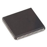
HD64F3337YCP16V Renesas Electronics America, HD64F3337YCP16V Datasheet - Page 293

HD64F3337YCP16V
Manufacturer Part Number
HD64F3337YCP16V
Description
MCU 3/5V 60K PB-FREE 84-PLCC
Manufacturer
Renesas Electronics America
Series
H8® H8/300r
Specifications of HD64F3337YCP16V
Core Size
8-Bit
Program Memory Size
60KB (60K x 8)
Oscillator Type
Internal
Core Processor
H8/300
Speed
16MHz
Connectivity
Host Interface, I²C, SCI
Peripherals
POR, PWM, WDT
Number Of I /o
74
Program Memory Type
FLASH
Ram Size
2K x 8
Voltage - Supply (vcc/vdd)
4.5 V ~ 5.5 V
Data Converters
A/D 8x10b; D/A 2x8b
Operating Temperature
-20°C ~ 75°C
Package / Case
84-PLCC
No. Of I/o's
74
Ram Memory Size
1KB
Cpu Speed
16MHz
No. Of Timers
6
No. Of Pwm Channels
2
Digital Ic Case Style
PLCC
Controller Family/series
H8/300
Rohs Compliant
Yes
Lead Free Status / RoHS Status
Lead free / RoHS Compliant
Eeprom Size
-
Lead Free Status / RoHS Status
Lead free / RoHS Compliant, Lead free / RoHS Compliant
Available stocks
Company
Part Number
Manufacturer
Quantity
Price
Company:
Part Number:
HD64F3337YCP16V
Manufacturer:
COILMASTER
Quantity:
30 000
Company:
Part Number:
HD64F3337YCP16V
Manufacturer:
Renesas Electronics America
Quantity:
10 000
- Current page: 293 of 749
- Download datasheet (4Mb)
Clock
In asynchronous mode it is possible to select either an internal clock created by the on-chip baud
rate generator, or an external clock input at the SCK pin. The selection is made by the C/A bit in
the serial mode register (SMR) and the CKE1 and CKE0 bits in the serial control register (SCR).
Refer to table 12.8.
If an external clock is input at the SCK pin, its frequency should be 16 times the desired bit rate.
If the internal clock provided by the on-chip baud rate generator is selected and the SCK pin is
used for clock output, the output clock frequency is equal to the bit rate, and the clock pulse rises
at the center of the transmit data bits. Figure 12.3 shows the phase relationship between the output
clock and transmit data.
Transmitting and Receiving Data
SCI Initialization: Before transmitting or receiving, software must clear the TE and RE bits to 0
in the serial control register (SCR), then initialize the SCI following the procedure in figure 12.4.
Note: When changing the communication mode or format, always clear the TE and RE bits to 0
before following the procedure given below. Clearing TE to 0 sets TDRE to 1 and
initializes the transmit shift register (TSR). Clearing RE to 0, however, does not initialize
the RDRF, PER, FER, and ORER flags and receive data register (RDR), which retain their
previous contents.
When an external clock is used, the clock should not be stopped during initialization or
subsequent operation. SCI operation becomes unreliable if the clock is stopped.
Figure 12.3 Phase Relationship between Clock Output and Transmit Data
0
D0
D1
D2
D3
(Asynchronous Mode)
One frame
D4
D5
D6
D7
0/1
1
1
261
Related parts for HD64F3337YCP16V
Image
Part Number
Description
Manufacturer
Datasheet
Request
R

Part Number:
Description:
KIT STARTER FOR M16C/29
Manufacturer:
Renesas Electronics America
Datasheet:

Part Number:
Description:
KIT STARTER FOR R8C/2D
Manufacturer:
Renesas Electronics America
Datasheet:

Part Number:
Description:
R0K33062P STARTER KIT
Manufacturer:
Renesas Electronics America
Datasheet:

Part Number:
Description:
KIT STARTER FOR R8C/23 E8A
Manufacturer:
Renesas Electronics America
Datasheet:

Part Number:
Description:
KIT STARTER FOR R8C/25
Manufacturer:
Renesas Electronics America
Datasheet:

Part Number:
Description:
KIT STARTER H8S2456 SHARPE DSPLY
Manufacturer:
Renesas Electronics America
Datasheet:

Part Number:
Description:
KIT STARTER FOR R8C38C
Manufacturer:
Renesas Electronics America
Datasheet:

Part Number:
Description:
KIT STARTER FOR R8C35C
Manufacturer:
Renesas Electronics America
Datasheet:

Part Number:
Description:
KIT STARTER FOR R8CL3AC+LCD APPS
Manufacturer:
Renesas Electronics America
Datasheet:

Part Number:
Description:
KIT STARTER FOR RX610
Manufacturer:
Renesas Electronics America
Datasheet:

Part Number:
Description:
KIT STARTER FOR R32C/118
Manufacturer:
Renesas Electronics America
Datasheet:

Part Number:
Description:
KIT DEV RSK-R8C/26-29
Manufacturer:
Renesas Electronics America
Datasheet:

Part Number:
Description:
KIT STARTER FOR SH7124
Manufacturer:
Renesas Electronics America
Datasheet:

Part Number:
Description:
KIT STARTER FOR H8SX/1622
Manufacturer:
Renesas Electronics America
Datasheet:

Part Number:
Description:
KIT DEV FOR SH7203
Manufacturer:
Renesas Electronics America
Datasheet:


