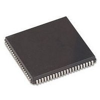
HD64F3337YCP16V Renesas Electronics America, HD64F3337YCP16V Datasheet - Page 98

HD64F3337YCP16V
Manufacturer Part Number
HD64F3337YCP16V
Description
MCU 3/5V 60K PB-FREE 84-PLCC
Manufacturer
Renesas Electronics America
Series
H8® H8/300r
Specifications of HD64F3337YCP16V
Core Size
8-Bit
Program Memory Size
60KB (60K x 8)
Oscillator Type
Internal
Core Processor
H8/300
Speed
16MHz
Connectivity
Host Interface, I²C, SCI
Peripherals
POR, PWM, WDT
Number Of I /o
74
Program Memory Type
FLASH
Ram Size
2K x 8
Voltage - Supply (vcc/vdd)
4.5 V ~ 5.5 V
Data Converters
A/D 8x10b; D/A 2x8b
Operating Temperature
-20°C ~ 75°C
Package / Case
84-PLCC
No. Of I/o's
74
Ram Memory Size
1KB
Cpu Speed
16MHz
No. Of Timers
6
No. Of Pwm Channels
2
Digital Ic Case Style
PLCC
Controller Family/series
H8/300
Rohs Compliant
Yes
Lead Free Status / RoHS Status
Lead free / RoHS Compliant
Eeprom Size
-
Lead Free Status / RoHS Status
Lead free / RoHS Compliant, Lead free / RoHS Compliant
Available stocks
Company
Part Number
Manufacturer
Quantity
Price
Company:
Part Number:
HD64F3337YCP16V
Manufacturer:
COILMASTER
Quantity:
30 000
Company:
Part Number:
HD64F3337YCP16V
Manufacturer:
Renesas Electronics America
Quantity:
10 000
- Current page: 98 of 749
- Download datasheet (4Mb)
Bit 0—RAM Enable (RAME): Enables or disables the on-chip RAM. The RAME bit is
initialized by a reset, but is not initialized in the software standby mode.
Bit 0: RAME
0
1
3.3
Notes: *1 H8/3337SF (S-mask model, single-power-supply on-chip flash memory version) only.
The mode control register (MDCR) is an 8-bit register that indicates the operating mode of the
chip.
Bit 7—Expanded Mode Enable (EXPE): Functions only in the H8/3337SF (S-mask model,
single-power-supply on-chip flash memory version). For details, see section 21.1.6, Mode Control
Register (MDCR).
In models other than the H8/3337SF, this is a reserved bit that cannot be modified and is always
read as 1.
Bits 6 and 5—Reserved: These bits cannot be modified and are always read as 1.
Bits 4 and 3—Reserved: These bits cannot be modified and are always read as 0.
Bit 2—Reserved: This bit cannot be modified and is always read as 1.
Bits 1 and 0—Mode Select 1 and 0 (MDS1 and MDS0): These bits indicate the values of the
mode pins (MD
corresponds to MD
control register is read, the levels at the mode pins (MD
3.4
Figures 3.1 to 3.3 show memory maps of the H8/3337Y, H8/3336Y, H8/3334Y, H8/3397,
H8/3396, and H8/3394 in modes 1, 2, and 3.
66
Bit
Initial value
Read/Write
*2 Determined by the mode pins (MD
Mode Control Register (MDCR)
Address Space Map in Each Operating Mode
Otherwise, this is a reserved bit that is always read as 1.
1
and MD
EXPE
R/W
1
—
Description
The on-chip RAM is disabled.
The on-chip RAM is enabled.
and MDS0 to MD
7
* 2
*2
*1
0
), thereby indicating the current operating mode of the chip. MDS1
—
—
6
1
0
. These bits can be read but not written. When the mode
—
—
5
1
1
and MD
—
—
4
0
0
).
1
and MD
—
—
3
0
0
) are latched in these bits.
—
—
2
1
MDS1
—
1
R
* 2
(Initial value)
MDS0
—
0
R
* 2
Related parts for HD64F3337YCP16V
Image
Part Number
Description
Manufacturer
Datasheet
Request
R

Part Number:
Description:
KIT STARTER FOR M16C/29
Manufacturer:
Renesas Electronics America
Datasheet:

Part Number:
Description:
KIT STARTER FOR R8C/2D
Manufacturer:
Renesas Electronics America
Datasheet:

Part Number:
Description:
R0K33062P STARTER KIT
Manufacturer:
Renesas Electronics America
Datasheet:

Part Number:
Description:
KIT STARTER FOR R8C/23 E8A
Manufacturer:
Renesas Electronics America
Datasheet:

Part Number:
Description:
KIT STARTER FOR R8C/25
Manufacturer:
Renesas Electronics America
Datasheet:

Part Number:
Description:
KIT STARTER H8S2456 SHARPE DSPLY
Manufacturer:
Renesas Electronics America
Datasheet:

Part Number:
Description:
KIT STARTER FOR R8C38C
Manufacturer:
Renesas Electronics America
Datasheet:

Part Number:
Description:
KIT STARTER FOR R8C35C
Manufacturer:
Renesas Electronics America
Datasheet:

Part Number:
Description:
KIT STARTER FOR R8CL3AC+LCD APPS
Manufacturer:
Renesas Electronics America
Datasheet:

Part Number:
Description:
KIT STARTER FOR RX610
Manufacturer:
Renesas Electronics America
Datasheet:

Part Number:
Description:
KIT STARTER FOR R32C/118
Manufacturer:
Renesas Electronics America
Datasheet:

Part Number:
Description:
KIT DEV RSK-R8C/26-29
Manufacturer:
Renesas Electronics America
Datasheet:

Part Number:
Description:
KIT STARTER FOR SH7124
Manufacturer:
Renesas Electronics America
Datasheet:

Part Number:
Description:
KIT STARTER FOR H8SX/1622
Manufacturer:
Renesas Electronics America
Datasheet:

Part Number:
Description:
KIT DEV FOR SH7203
Manufacturer:
Renesas Electronics America
Datasheet:


