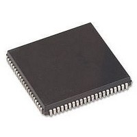
HD64F3337YCP16V Renesas Electronics America, HD64F3337YCP16V Datasheet - Page 541

HD64F3337YCP16V
Manufacturer Part Number
HD64F3337YCP16V
Description
MCU 3/5V 60K PB-FREE 84-PLCC
Manufacturer
Renesas Electronics America
Series
H8® H8/300r
Specifications of HD64F3337YCP16V
Core Size
8-Bit
Program Memory Size
60KB (60K x 8)
Oscillator Type
Internal
Core Processor
H8/300
Speed
16MHz
Connectivity
Host Interface, I²C, SCI
Peripherals
POR, PWM, WDT
Number Of I /o
74
Program Memory Type
FLASH
Ram Size
2K x 8
Voltage - Supply (vcc/vdd)
4.5 V ~ 5.5 V
Data Converters
A/D 8x10b; D/A 2x8b
Operating Temperature
-20°C ~ 75°C
Package / Case
84-PLCC
No. Of I/o's
74
Ram Memory Size
1KB
Cpu Speed
16MHz
No. Of Timers
6
No. Of Pwm Channels
2
Digital Ic Case Style
PLCC
Controller Family/series
H8/300
Rohs Compliant
Yes
Lead Free Status / RoHS Status
Lead free / RoHS Compliant
Eeprom Size
-
Lead Free Status / RoHS Status
Lead free / RoHS Compliant, Lead free / RoHS Compliant
Available stocks
Company
Part Number
Manufacturer
Quantity
Price
Company:
Part Number:
HD64F3337YCP16V
Manufacturer:
COILMASTER
Quantity:
30 000
Company:
Part Number:
HD64F3337YCP16V
Manufacturer:
Renesas Electronics America
Quantity:
10 000
- Current page: 541 of 749
- Download datasheet (4Mb)
Bit 4—Flash Memory Control Register Enable (FLSHE): When the FLSHE bit is set to 1, the
flash memory control registers can be read and written to. When FLSHE is cleared to 0, the flash
memory control registers are unselected. In this case, the contents of the flash memory contents
are retained.
Bit 4: FLSHE
0
1
Bits 3 and 2—Wait Mode Select 1 and 0 (WMS1, WMS0)
Bits 1 and 0—Wait Count 1 and 0 (WC1, WC0)
These bits control insertion of wait states by the wait-state controller. For details, see section 5,
Wait-State Controller.
21.3
When an on-board programming mode is selected, the on-chip flash memory can be programmed,
erased, and verified. There are two on-board programming modes: boot mode and user
programming mode. Table 21.6 indicates how to select the on-board programming modes. User
programming mode operation can be performed by setting control bits with software. A state
transition diagram for flash memory related modes is shown in figure 21.2.
Table 21.6 On-Board Programming Mode Selection
Mode Selection
Boot mode
User programming
mode
21.3.1
To use boot mode, a user program for programming and erasing the flash memory must be
provided in advance on the host machine (which may be a personal computer). Serial
communication interface (SCI) channel 1 is used in asynchronous mode.
When a reset state is executed after the H8/3337SF pins have been set to boot mode, the built-in
boot program is activated, and the on-board update routine provided in the host is transferred
sequentially to the H8/3337SF using the serial communication interface (SCI). The H8/3337SF
writes the on-board update routine received via the SCI to the on-board update routine area in the
on-chip RAM. After the transfer is completed, execution branches to the first address of the on-
On-Board Programming Modes
Boot Mode
Description
Flash memory control registers are in unselected state
Flash memory control registers are in selected state
MD
0
1
1
MD
0
0
1
0
P9
1
—
2
P9
1
—
1
P9
1
—
(Initial value)
0
509
Related parts for HD64F3337YCP16V
Image
Part Number
Description
Manufacturer
Datasheet
Request
R

Part Number:
Description:
KIT STARTER FOR M16C/29
Manufacturer:
Renesas Electronics America
Datasheet:

Part Number:
Description:
KIT STARTER FOR R8C/2D
Manufacturer:
Renesas Electronics America
Datasheet:

Part Number:
Description:
R0K33062P STARTER KIT
Manufacturer:
Renesas Electronics America
Datasheet:

Part Number:
Description:
KIT STARTER FOR R8C/23 E8A
Manufacturer:
Renesas Electronics America
Datasheet:

Part Number:
Description:
KIT STARTER FOR R8C/25
Manufacturer:
Renesas Electronics America
Datasheet:

Part Number:
Description:
KIT STARTER H8S2456 SHARPE DSPLY
Manufacturer:
Renesas Electronics America
Datasheet:

Part Number:
Description:
KIT STARTER FOR R8C38C
Manufacturer:
Renesas Electronics America
Datasheet:

Part Number:
Description:
KIT STARTER FOR R8C35C
Manufacturer:
Renesas Electronics America
Datasheet:

Part Number:
Description:
KIT STARTER FOR R8CL3AC+LCD APPS
Manufacturer:
Renesas Electronics America
Datasheet:

Part Number:
Description:
KIT STARTER FOR RX610
Manufacturer:
Renesas Electronics America
Datasheet:

Part Number:
Description:
KIT STARTER FOR R32C/118
Manufacturer:
Renesas Electronics America
Datasheet:

Part Number:
Description:
KIT DEV RSK-R8C/26-29
Manufacturer:
Renesas Electronics America
Datasheet:

Part Number:
Description:
KIT STARTER FOR SH7124
Manufacturer:
Renesas Electronics America
Datasheet:

Part Number:
Description:
KIT STARTER FOR H8SX/1622
Manufacturer:
Renesas Electronics America
Datasheet:

Part Number:
Description:
KIT DEV FOR SH7203
Manufacturer:
Renesas Electronics America
Datasheet:


