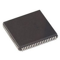
HD64F3337YCP16V Renesas Electronics America, HD64F3337YCP16V Datasheet - Page 522

HD64F3337YCP16V
Manufacturer Part Number
HD64F3337YCP16V
Description
MCU 3/5V 60K PB-FREE 84-PLCC
Manufacturer
Renesas Electronics America
Series
H8® H8/300r
Specifications of HD64F3337YCP16V
Core Size
8-Bit
Program Memory Size
60KB (60K x 8)
Oscillator Type
Internal
Core Processor
H8/300
Speed
16MHz
Connectivity
Host Interface, I²C, SCI
Peripherals
POR, PWM, WDT
Number Of I /o
74
Program Memory Type
FLASH
Ram Size
2K x 8
Voltage - Supply (vcc/vdd)
4.5 V ~ 5.5 V
Data Converters
A/D 8x10b; D/A 2x8b
Operating Temperature
-20°C ~ 75°C
Package / Case
84-PLCC
No. Of I/o's
74
Ram Memory Size
1KB
Cpu Speed
16MHz
No. Of Timers
6
No. Of Pwm Channels
2
Digital Ic Case Style
PLCC
Controller Family/series
H8/300
Rohs Compliant
Yes
Lead Free Status / RoHS Status
Lead free / RoHS Compliant
Eeprom Size
-
Lead Free Status / RoHS Status
Lead free / RoHS Compliant, Lead free / RoHS Compliant
Available stocks
Company
Part Number
Manufacturer
Quantity
Price
Company:
Part Number:
HD64F3337YCP16V
Manufacturer:
COILMASTER
Quantity:
30 000
Company:
Part Number:
HD64F3337YCP16V
Manufacturer:
Renesas Electronics America
Quantity:
10 000
- Current page: 522 of 749
- Download datasheet (4Mb)
(7) Design a current margin into the programming voltage (V
V
Programming and erasing may become impossible outside this range.
(8) Ensure that peak overshoot does not exceed the rated value at the FV
Connect decoupling capacitors as close to the FV
Also connect decoupling capacitors to the MD
(9) Use the recommended algorithms for programming and erasing flash memory. These
algorithms are designed to program and erase without subjecting the device to voltage stress and
without sacrificing the reliability of programmed data.
Before setting the program (P) or erase (E) bit in the flash memory control register (FLMCR), set
the watchdog timer to ensure that the P or E bit does not remain set for more than the specified
time.
(10) For details on interrupt handling while flash memory is being programmed or erased,
see the notes on NMI interrupt handling in section 20.4.9, Interrupt Handling during Flash
Memory Programming and Erasing.
(11) Cautions on Accessing Flash Memory Control Registers
1. Flash memory control register access state in each operating mode
490
PP
The H8/3337YF has flash memory control registers located at addresses H'FF80 (FLMCR),
H'FF82 (EBR1), and H'FF83 (EBR2). These registers can only be accessed when 12 V is
applied to the flash memory program power supply pin, FV
Table 1 shows the area accessed for the above addresses in each mode, when 12 V is and is not
applied to FV
will not depart from 12.0 0.6 V (11.4 V to 12.6 V) during programming or erasing.
12 V
PP
Figure 20.21 V
.
1.0 F
PP
Power Supply Circuit Design (Example)
0.01 F
1
pin in the same way when boot mode is uesd.
PP
and MD
FV
1
pins as possible.
PP
PP
.
PP
) power supply. Ensure that
H8/3337YF
PP
and MD
1
pins.
Related parts for HD64F3337YCP16V
Image
Part Number
Description
Manufacturer
Datasheet
Request
R

Part Number:
Description:
KIT STARTER FOR M16C/29
Manufacturer:
Renesas Electronics America
Datasheet:

Part Number:
Description:
KIT STARTER FOR R8C/2D
Manufacturer:
Renesas Electronics America
Datasheet:

Part Number:
Description:
R0K33062P STARTER KIT
Manufacturer:
Renesas Electronics America
Datasheet:

Part Number:
Description:
KIT STARTER FOR R8C/23 E8A
Manufacturer:
Renesas Electronics America
Datasheet:

Part Number:
Description:
KIT STARTER FOR R8C/25
Manufacturer:
Renesas Electronics America
Datasheet:

Part Number:
Description:
KIT STARTER H8S2456 SHARPE DSPLY
Manufacturer:
Renesas Electronics America
Datasheet:

Part Number:
Description:
KIT STARTER FOR R8C38C
Manufacturer:
Renesas Electronics America
Datasheet:

Part Number:
Description:
KIT STARTER FOR R8C35C
Manufacturer:
Renesas Electronics America
Datasheet:

Part Number:
Description:
KIT STARTER FOR R8CL3AC+LCD APPS
Manufacturer:
Renesas Electronics America
Datasheet:

Part Number:
Description:
KIT STARTER FOR RX610
Manufacturer:
Renesas Electronics America
Datasheet:

Part Number:
Description:
KIT STARTER FOR R32C/118
Manufacturer:
Renesas Electronics America
Datasheet:

Part Number:
Description:
KIT DEV RSK-R8C/26-29
Manufacturer:
Renesas Electronics America
Datasheet:

Part Number:
Description:
KIT STARTER FOR SH7124
Manufacturer:
Renesas Electronics America
Datasheet:

Part Number:
Description:
KIT STARTER FOR H8SX/1622
Manufacturer:
Renesas Electronics America
Datasheet:

Part Number:
Description:
KIT DEV FOR SH7203
Manufacturer:
Renesas Electronics America
Datasheet:


