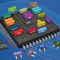
CY8C3866AXI-040 Cypress Semiconductor Corp, CY8C3866AXI-040 Datasheet - Page 24

CY8C3866AXI-040
Manufacturer Part Number
CY8C3866AXI-040
Description
PSOC 3 TQFP
Manufacturer
Cypress Semiconductor Corp
Series
PSOC™ 3 CY8C38xxr
Datasheet
1.CY8C3865LTI-058.pdf
(129 pages)
Specifications of CY8C3866AXI-040
Package / Case
*
Voltage - Supply (vcc/vdd)
1.71 V ~ 5.5 V
Operating Temperature
-40°C ~ 85°C
Speed
67MHz
Number Of I /o
62
Eeprom Size
2K x 8
Core Processor
8051
Program Memory Type
FLASH
Ram Size
8K x 8
Program Memory Size
64KB (64K x 8)
Data Converters
A/D 2x20b, D/A 4x8b
Oscillator Type
Internal
Peripherals
CapSense, DMA, LCD, POR, PWM, WDT
Connectivity
CAN, EBI/EMI, I²C, LIN, SPI, UART/USART, USB
Core Size
8-Bit
Processor Series
CY8C38
Core
8051
Data Bus Width
32 bit
Data Ram Size
8 KB
Interface Type
I2C, SPI, UART, USB
Maximum Clock Frequency
67 MHz
Number Of Programmable I/os
28 to 72
Number Of Timers
4
Operating Supply Voltage
0.5 V to 5.5 V
Maximum Operating Temperature
+ 85 C
Mounting Style
SMD/SMT
Controller Family/series
(8051) PSOC 3
No. Of I/o's
62
Eeprom Memory Size
2KB
Ram Memory Size
8KB
Cpu Speed
67MHz
Lead Free Status / RoHS Status
Lead free / RoHS Compliant
Lead Free Status / RoHS Status
Lead free / RoHS Compliant
Available stocks
Company
Part Number
Manufacturer
Quantity
Price
Company:
Part Number:
CY8C3866AXI-040
Manufacturer:
Cypress Semiconductor
Quantity:
135
Company:
Part Number:
CY8C3866AXI-040
Manufacturer:
NXP
Quantity:
112
Company:
Part Number:
CY8C3866AXI-040
Manufacturer:
Cypress Semiconductor Corp
Quantity:
10 000
Part Number:
CY8C3866AXI-040
Manufacturer:
CYPRESS/赛普拉斯
Quantity:
20 000
Company:
Part Number:
CY8C3866AXI-040ES2
Manufacturer:
CYPRESS
Quantity:
153
5.7 Memory Map
The CY8C38 8051 memory map is very similar to the MCS-51
memory map.
5.7.1 Code Space
The CY8C38 8051 code space is 64 KB. Only main flash exists
in this space. See the
5.7.2 Internal Data Space
The CY8C38 8051 internal data space is 384 bytes, compressed
within a 256-byte space. This space consists of 256 bytes of
RAM (in addition to the SRAM mentioned in
21) and a 128-byte space for special function registers (SFR).
See
registers R0-R7. The next 16 bytes are bit-addressable.
5.7.3 SFRs
The SFR space provides access to frequently accessed registers. The memory map for the SFR memory space is shown in
Table 5-4. SFR Map
The CY8C38 family provides the standard set of registers found
on industry standard 8051 devices. In addition, the CY8C38
devices add SFRs to provide direct access to the I/O ports on the
device. The following sections describe the SFRs added to the
CY8C38 family.
XData Space Access SFRs
The 8051 core features dual DPTR registers for faster data
transfer operations. The data pointer select SFR, DPS, selects
Document Number: 001-11729 Rev. *R
Address
0×D8
0×D0
0×C8
0×C0
0×F8
0×F0
0×E8
0×E0
0×B8
0×B0
0×A8
0×A0
0×98
0×90
0×88
0×80
Figure
SFRPRT15DR
B
SFRPRT12DR
ACC
SFRPRT6DR
PSW
SFRPRT5DR
SFRPRT4DR
SFRPRT3DR
IE
P2AX
SFRPRT2DR
SFRPRT1DR
–
SFRPRT0DR
5-2. The lowest 32 bytes are used for 4 banks of
0/8
Flash Program Memory
SFRPRT15PS
–
SFRPRT12PS
–
SFRPRT6PS
–
SFRPRT5PS
SFRPRT4PS
SFRPRT3PS
–
–
SFRPRT2PS
SFRPRT1PS
SFRPRT0PS
SP
1/9
Static RAM
on page 21.
SFRPRT15SEL
SFRPRT12SEL
MXAX
–
SFRPRT6SEL
–
SFRPRT5SEL
SFRPRT4SEL
SFRPRT3SEL
–
SFRPRT1SEL
SFRPRT2SEL
–
SFRPRT0SEL
DPL0
on page
2/A
Figure 5-2. 8051 Internal Data Space
In addition to the register or bit address modes used with the
lower 48 bytes, the lower 128 bytes can be accessed with direct
or indirect addressing. With direct addressing mode, the upper
128 bytes map to the SFRs. With indirect addressing mode, the
upper 128 bytes map to RAM. Stack operations use indirect
addressing; the 8051 stack space is 256 bytes. See the
“Addressing Modes”
which data pointer register, DPTR0 or DPTR1, is used for the
following instructions:
–
–
–
–
–
–
–
–
–
–
–
–
–
DPX0
–
DPH0
MOVX @DPTR, A
MOVX A, @DPTR
MOVC A, @A+DPTR
JMP @A+DPTR
0x1F
0x2F
0x7F
0xFF
0x00
0x20
0x30
0x80
3/B
Upper Core RAM Shared
–
–
–
–
–
–
–
–
–
–
–
–
–
–
–
DPL1
(indirect addressing)
with Stack Space
4/C
Lower Core RAM Shared with Stack Space
PSoC
section on page 11.
(direct and indirect addressing)
–
–
–
–
–
–
–
–
–
–
–
–
–
DPX1
–
DPH1
4 Banks, R0-R7 Each
Bit-Addressable Area
®
5/D
3: CY8C38 Family
Special Function Registers
–
–
–
–
–
–
–
–
–
–
–
–
–
–
–
DPS
(direct addressing)
6/E
Data Sheet
SFR
Page 24 of 129
–
–
–
–
–
–
–
–
–
–
–
–
–
–
–
–
Table
7/F
5-4.
[+] Feedback


