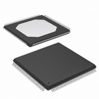
XCV50-6TQ144C Xilinx Inc, XCV50-6TQ144C Datasheet - Page 10

XCV50-6TQ144C
Manufacturer Part Number
XCV50-6TQ144C
Description
IC FPGA 2.5V C-TEMP 144-TQFP
Manufacturer
Xilinx Inc
Series
Virtex™r
Datasheet
1.XCV100-5PQ240C.pdf
(76 pages)
Specifications of XCV50-6TQ144C
Number Of Logic Elements/cells
1728
Number Of Labs/clbs
384
Total Ram Bits
32768
Number Of I /o
98
Number Of Gates
57906
Voltage - Supply
2.375 V ~ 2.625 V
Mounting Type
Surface Mount
Operating Temperature
0°C ~ 85°C
Package / Case
144-LQFP
Case
TQFP144
Dc
03+
Lead Free Status / RoHS Status
Contains lead / RoHS non-compliant
Available stocks
Company
Part Number
Manufacturer
Quantity
Price
Company:
Part Number:
XCV50-6TQ144C
Manufacturer:
XIL
Quantity:
1 238
Company:
Part Number:
XCV50-6TQ144C
Manufacturer:
XILINX
Quantity:
988
Virtex™ 2.5 V Field Programmable Gate Arrays
Each block SelectRAM cell, as illustrated in
fully synchronous dual-ported 4096-bit RAM with indepen-
dent control signals for each port. The data widths of the
two ports can be configured independently, providing
built-in bus-width conversion.
Table 4
block SelectRAM.
Local Routing
The VersaBlock provides local routing resources, as shown
in
tions.
•
Module 2 of 4
6
Figure
Interconnections among the LUTs, flip-flops, and GRM
shows the depth and width aspect ratios for the
Figure 6: Dual-Port Block SelectRAM
7, providing the following three types of connec-
WEA
ENA
RSTA
ADDRA[#:0]
DIA[#:0]
WEB
ENB
RSTB
ADDRB[#:0]
DIB[#:0]
CLKA
CLKB
RAMB4_S#_S#
To Adjacent
X8794b
GRM
DOA[#:0]
DOB[#:0]
Direct Connection
xcv_ds_006
To Adjacent
To Adjacent
To Adjacent
GRM
GRM
Figure 7: Virtex Local Routing
GRM
Figure
CLB
6, is a
www.xilinx.com
1-800-255-7778
To Adjacent
GRM
Table 4: Block SelectRAM Port Aspect Ratios
The Virtex block SelectRAM also includes dedicated routing
to provide an efficient interface with both CLBs and other
block SelectRAMs. Refer to XAPP130 for block SelectRAM
timing waveforms.
Programmable Routing Matrix
It is the longest delay path that limits the speed of any
worst-case design. Consequently, the Virtex routing archi-
tecture and its place-and-route software were defined in a
single optimization process. This joint optimization mini-
mizes long-path delays, and consequently, yields the best
system performance.
The joint optimization also reduces design compilation
times because the architecture is software-friendly. Design
cycles are correspondingly reduced due to shorter design
iteration times.
•
•
Width
Internal CLB feedback paths that provide high-speed
connections to LUTs within the same CLB, chaining
them together with minimal routing delay
Direct paths that provide high-speed connections
between horizontally adjacent CLBs, eliminating the
delay of the GRM.
16
1
2
4
8
CLB
Depth
4096
2048
1024
512
256
Direct Connection
To Adjacent
CLB
ADDR<11:0>
ADDR<10:0>
DS003-2 (v2.8.1) December 9, 2002
ADDR<9:0>
ADDR<8:0>
ADDR<7:0>
ADDR Bus
Product Specification
DATA<15:0>
DATA<1:0>
DATA<3:0>
DATA<7:0>
Data Bus
DATA<0>
R


