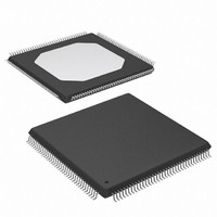
XCV50-6TQ144C Xilinx Inc, XCV50-6TQ144C Datasheet - Page 2

XCV50-6TQ144C
Manufacturer Part Number
XCV50-6TQ144C
Description
IC FPGA 2.5V C-TEMP 144-TQFP
Manufacturer
Xilinx Inc
Series
Virtex™r
Datasheet
1.XCV100-5PQ240C.pdf
(76 pages)
Specifications of XCV50-6TQ144C
Number Of Logic Elements/cells
1728
Number Of Labs/clbs
384
Total Ram Bits
32768
Number Of I /o
98
Number Of Gates
57906
Voltage - Supply
2.375 V ~ 2.625 V
Mounting Type
Surface Mount
Operating Temperature
0°C ~ 85°C
Package / Case
144-LQFP
Case
TQFP144
Dc
03+
Lead Free Status / RoHS Status
Contains lead / RoHS non-compliant
Available stocks
Company
Part Number
Manufacturer
Quantity
Price
Company:
Part Number:
XCV50-6TQ144C
Manufacturer:
XIL
Quantity:
1 238
Company:
Part Number:
XCV50-6TQ144C
Manufacturer:
XILINX
Quantity:
988
Virtex™ 2.5 V Field Programmable Gate Arrays
Virtex Architecture
Virtex devices feature a flexible, regular architecture that
comprises an array of configurable logic blocks (CLBs) sur-
rounded by programmable input/output blocks (IOBs), all
interconnected by a rich hierarchy of fast, versatile routing
resources. The abundance of routing resources permits the
Virtex family to accommodate even the largest and most
complex designs.
Virtex FPGAs are SRAM-based, and are customized by
loading configuration data into internal memory cells. In
some modes, the FPGA reads its own configuration data
from an external PROM (master serial mode). Otherwise,
the configuration data is written into the FPGA (Select-
MAP™, slave serial, and JTAG modes).
The standard Xilinx Foundation™ and Alliance Series™
Development systems deliver complete design support for
Virtex, covering every aspect from behavioral and sche-
matic entry, through simulation, automatic design transla-
tion and implementation, to the creation, downloading, and
readback of a configuration bit stream.
Higher Performance
Virtex devices provide better performance than previous
generations of FPGA. Designs can achieve synchronous
system clock rates up to 200 MHz including I/O. Virtex
inputs and outputs comply fully with PCI specifications, and
interfaces can be implemented that operate at 33 MHz or 66
MHz. Additionally, Virtex supports the hot-swapping
requirements of Compact PCI.
Module 1 of 4
2
www.xilinx.com
1-800-255-7778
Xilinx thoroughly benchmarked the Virtex family. While per-
formance is design-dependent, many designs operated
internally at speeds in excess of 100 MHz and can achieve
200 MHz.
tive circuits, using worst-case timing parameters.
Table 2: Performance for Common Circuit Functions
Pipelined Multiplier
Address Decoder
16:1 Multiplexer
Parity Tree
Chip-to-Chip
HSTL Class IV
LVTTL,16mA, fast slew
Register-to-Register
Function
Adder
Table 2
shows performance data for representa-
16 x 16
8 x 8
Bits
16
64
16
64
18
36
9
DS003-1 (v2.5 ) April 2, 2001
Product Specification
Virtex -6
200 MHz
180 MHz
5.0 ns
7.2 ns
5.1 ns
6.0 ns
4.4 ns
6.4 ns
5.4 ns
4.1 ns
5.0 ns
6.9 ns
R


