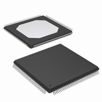
XCV50-6TQ144C Xilinx Inc, XCV50-6TQ144C Datasheet - Page 24

XCV50-6TQ144C
Manufacturer Part Number
XCV50-6TQ144C
Description
IC FPGA 2.5V C-TEMP 144-TQFP
Manufacturer
Xilinx Inc
Series
Virtex™r
Datasheet
1.XCV100-5PQ240C.pdf
(76 pages)
Specifications of XCV50-6TQ144C
Number Of Logic Elements/cells
1728
Number Of Labs/clbs
384
Total Ram Bits
32768
Number Of I /o
98
Number Of Gates
57906
Voltage - Supply
2.375 V ~ 2.625 V
Mounting Type
Surface Mount
Operating Temperature
0°C ~ 85°C
Package / Case
144-LQFP
Case
TQFP144
Dc
03+
Lead Free Status / RoHS Status
Contains lead / RoHS non-compliant
Available stocks
Company
Part Number
Manufacturer
Quantity
Price
Company:
Part Number:
XCV50-6TQ144C
Manufacturer:
XIL
Quantity:
1 238
Company:
Part Number:
XCV50-6TQ144C
Manufacturer:
XILINX
Quantity:
988
Virtex™ 2.5 V Field Programmable Gate Arrays
Virtex Data Sheet
The Virtex Data Sheet contains the following modules:
•
•
Module 2 of 4
20
07/19/01
07/19/02
09/10/02
12/09/02
DS003-1, Virtex 2.5V FPGAs:
Introduction and Ordering Information (Module 1)
DS003-2, Virtex 2.5V FPGAs:
Functional Description (Module 2)
01/00
03/00
05/00
05/00
09/00
10/00
04/01
Date
Version
2.8.1
1.9
2.0
2.1
2.2
2.3
2.4
2.5
2.6
2.7
2.8
•
•
•
•
•
•
•
•
•
•
•
•
•
Updated DLL Jitter Parameter table and waveforms, added Delay Measurement
Methodology table for different I/O standards, changed buffered Hex line info and
Input/Output Timing measurement notes.
New TBCKO values; corrected FG680 package connection drawing; new note about status
of CCLK pin after configuration.
Modified “Pins not listed ...” statement. Speed grade update to Final status.
Modified Table 18.
Added XCV400 values to table under Minimum Clock-to-Out for Virtex Devices.
Corrected Units column in table under IOB Input Switching Characteristics.
Added values to table under CLB SelectRAM Switching Characteristics.
Corrected Pinout information for devices in the BG256, BG432, and BG560 packages in
Table 18.
Corrected BG256 Pin Function Diagram.
Revised minimums for Global Clock Set-Up and Hold for LVTTL Standard, with DLL.
Updated SelectMAP Write Timing Characteristics values in
Converted file to modularized format. See the
Made minor edits to text under Configuration.
Made minor edit to
Added clarifications in the Configuration,
SelectRAM
Added clarification in the
Corrected number of buffered Hex lines listed in
sections. Revised
www.xilinx.com
Figure 16
1-800-255-7778
Boundary Scan
•
•
and
Figure
DS003-3, Virtex 2.5V FPGAs:
DC and Switching Characteristics (Module 3)
DS003-4, Virtex 2.5V FPGAs:
Pinout Tables (Module 4)
Figure
Revision
17.
18.
Boundary-Scan
section.
Virtex Data Sheet
General Purpose Routing
DS003-2 (v2.8.1) December 9, 2002
Table
Mode, and
9.
section.
Product Specification
Block
section.
R


