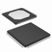
XCV50-6TQ144C Xilinx Inc, XCV50-6TQ144C Datasheet - Page 22

XCV50-6TQ144C
Manufacturer Part Number
XCV50-6TQ144C
Description
IC FPGA 2.5V C-TEMP 144-TQFP
Manufacturer
Xilinx Inc
Series
Virtex™r
Datasheet
1.XCV100-5PQ240C.pdf
(76 pages)
Specifications of XCV50-6TQ144C
Number Of Logic Elements/cells
1728
Number Of Labs/clbs
384
Total Ram Bits
32768
Number Of I /o
98
Number Of Gates
57906
Voltage - Supply
2.375 V ~ 2.625 V
Mounting Type
Surface Mount
Operating Temperature
0°C ~ 85°C
Package / Case
144-LQFP
Case
TQFP144
Dc
03+
Lead Free Status / RoHS Status
Contains lead / RoHS non-compliant
Available stocks
Company
Part Number
Manufacturer
Quantity
Price
Company:
Part Number:
XCV50-6TQ144C
Manufacturer:
XIL
Quantity:
1 238
Company:
Part Number:
XCV50-6TQ144C
Manufacturer:
XILINX
Quantity:
988
Virtex™ 2.5 V Field Programmable Gate Arrays
Boundary-Scan Mode
In the boundary-scan mode, configuration is done through
the IEEE 1149.1 Test Access Port. Note that the
PROGRAM pin must be pulled High prior to reconfiguration.
A Low on the PROGRAM pin resets the TAP controller and
no JTAG operations can be performed.
Configuration through the TAP uses the CFG_IN instruc-
tion. This instruction allows data input on TDI to be con-
verted into data packets for the internal configuration bus.
The following steps are required to configure the FPGA
through the boundary-scan port (when using TCK as a
start-up clock).
1. Load the CFG_IN instruction into the boundary-scan
2. Enter the Shift-DR (SDR) state
3. Shift a configuration bitstream into TDI
4. Return to Run-Test-Idle (RTI)
5. Load the JSTART instruction into IR
6. Enter the SDR state
7. Clock TCK through the startup sequence
8. Return to RTI
Configuration and readback via the TAP is always available.
The boundary-scan mode is selected by a <101> or 001>
on the mode pins (M2, M1, M0). For details on TAP charac-
teristics, refer to XAPP139.
Configuration Sequence
The configuration of Virtex devices is a three-phase pro-
cess. First, the configuration memory is cleared. Next, con-
figuration data is loaded into the memory, and finally, the
logic is activated by a start-up process.
Configuration is automatically initiated on power-up unless
it is delayed by the user, as described below. The configura-
tion process can also be initiated by asserting PROGRAM.
Module 2 of 4
18
DATA[0:7]
WRITE
instruction register (IR)
CCLK
BUSY
Figure 18: SelectMAP Write Abort Waveforms
CS
Abort
X8797_c
www.xilinx.com
1-800-255-7778
The end of the memory-clearing phase is signalled by INIT
going High, and the completion of the entire process is sig-
nalled by DONE going High.
The power-up timing of configuration signals is shown in
Figure
listed in
Table 10: Power-up Timing Characteristics
Delaying Configuration
INIT can be held Low using an open-drain driver. An
open-drain is required since INIT is a bidirectional
open-drain pin that is held Low by the FPGA while the con-
figuration memory is being cleared. Extending the time that
the pin is Low causes the configuration sequencer to wait.
Thus, configuration is delayed by preventing entry into the
phase where data is loaded.
Start-Up Sequence
The default Start-up sequence is that one CCLK cycle after
DONE goes High, the global 3-state signal (GTS) is released.
This permits device outputs to turn on as necessary.
One CCLK cycle later, the Global Set/Reset (GSR) and Glo-
bal Write Enable (GWE) signals are released. This permits
the internal storage elements to begin changing state in
response to the logic and the user clock.
The relative timing of these events can be changed. In addi-
tion, the GTS, GSR, and GWE events can be made depen-
dent on the DONE pins of multiple devices all going High,
forcing the devices to start in synchronism. The sequence
can also be paused at any stage until lock has been
achieved on any or all DLLs.
Power-on Reset
Program Latency
CCLK (output) Delay
Program Pulse Width
Figure 19: Power-Up Timing Configuration Signals
PROGRAM
V
Description
INIT
CC
19. The corresponding timing characteristics are
Table
10.
CCLK OUTPUT or INPUT
T
POR
T
DS003-2 (v2.8.1) December 9, 2002
Symbol
PROGRAM
M0, M1, M2
(Required)
T
T
T
ICCK
T
POR
PI
PL
Product Specification
Value
100.0
300
VALID
2.0
0.5
4.0
T
ICCK
ms, max
µ
µ
µ
ns, min
Units
s, max
s, max
s, min
98122302
R


