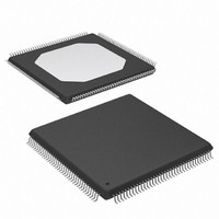
XCV50-6TQ144C Xilinx Inc, XCV50-6TQ144C Datasheet - Page 18

XCV50-6TQ144C
Manufacturer Part Number
XCV50-6TQ144C
Description
IC FPGA 2.5V C-TEMP 144-TQFP
Manufacturer
Xilinx Inc
Series
Virtex™r
Datasheet
1.XCV100-5PQ240C.pdf
(76 pages)
Specifications of XCV50-6TQ144C
Number Of Logic Elements/cells
1728
Number Of Labs/clbs
384
Total Ram Bits
32768
Number Of I /o
98
Number Of Gates
57906
Voltage - Supply
2.375 V ~ 2.625 V
Mounting Type
Surface Mount
Operating Temperature
0°C ~ 85°C
Package / Case
144-LQFP
Case
TQFP144
Dc
03+
Lead Free Status / RoHS Status
Contains lead / RoHS non-compliant
Available stocks
Company
Part Number
Manufacturer
Quantity
Price
Company:
Part Number:
XCV50-6TQ144C
Manufacturer:
XIL
Quantity:
1 238
Company:
Part Number:
XCV50-6TQ144C
Manufacturer:
XILINX
Quantity:
988
Virtex™ 2.5 V Field Programmable Gate Arrays
Master-Serial Mode
In master-serial mode, the CCLK output of the FPGA drives
a Xilinx Serial PROM that feeds bit-serial data to the DIN
input. The FPGA accepts this data on each rising CCLK
edge. After the FPGA has been loaded, the data for the next
device in a daisy-chain is presented on the DOUT pin after
the rising CCLK edge.
The interface is identical to slave-serial except that an inter-
nal oscillator is used to generate the configuration clock
(CCLK). A wide range of frequencies can be selected for
CCLK which always starts at a slow default frequency. Con-
figuration bits then switch CCLK to a higher frequency for
the remainder of the configuration. Switching to a lower fre-
quency is prohibited.
The CCLK frequency is set using the ConfigRate option in
the bitstream generation software. The maximum CCLK fre-
quency that can be selected is 60 MHz. When selecting a
CCLK frequency, ensure that the serial PROM and any
At power-up, V
than 50 ms, otherwise delay configuration by pulling
PROGRAM Low until V
The sequence of operations necessary to configure a Virtex
FPGA serially appears in
SelectMAP Mode
The SelectMAP mode is the fastest configuration option.
Byte-wide data is written into the FPGA with a BUSY flag
controlling the flow of data.
An external data source provides a byte stream, CCLK, a
Chip Select (CS) signal and a Write signal (WRITE). If
BUSY is asserted (High) by the FPGA, the data must be
held until BUSY goes Low.
Data can also be read using the SelectMAP mode. If
WRITE is not asserted, configuration data is read out of the
FPGA as part of a readback operation.
Module 2 of 4
14
Serial Data In
Serial DOUT
(Output)
(Output)
CC
CCLK
must rise from 1.0 V to V
Figure 14: Master-Serial Mode Programming Switching Characteristics
CC
Figure
is valid.
15.
T CKDS
1 T DSCK
2
CC
min in less
www.xilinx.com
1-800-255-7778
daisy-chained FPGAs are fast enough to support the clock
rate.
On power-up, the CCLK frequency is 2.5 MHz. This fre-
quency is used until the ConfigRate bits have been loaded
when the frequency changes to the selected ConfigRate.
Unless a different frequency is specified in the design, the
default ConfigRate is 4 MHz.
Figure 12
the left-most device operates in master-serial mode. The
remaining devices operate in slave-serial mode. The
SPROM RESET pin is driven by INIT, and the CE input is
driven by DONE. There is the potential for contention on the
DONE pin, depending on the start-up sequence options
chosen.
Figure 14
Master-serial mode is selected by a <000> or <100> on the
mode pins (M2, M1, M0).
tion for
In the SelectMAP mode, multiple Virtex devices can be
chained in parallel. DATA pins (D7:D0), CCLK, WRITE,
BUSY, PROGRAM, DONE, and INIT can be connected in
parallel between all the FPGAs. Note that the data is orga-
nized with the MSB of each byte on pin DO and the LSB of
each byte on D7. The CS pins are kept separate, insuring
that each FPGA can be selected individually. WRITE should
be Low before loading the first bitstream and returned High
after the last device has been programmed. Use CS to
select the appropriate FPGA for loading the bitstream and
sending the configuration data. at the end of the bitstream,
deselect the loaded device and select the next target FPGA
by setting its CS pin High. A free-running oscillator or other
externally generated signal can be used for CCLK. The
BUSY signal can be ignored for frequencies below 50 MHz.
For details about frequencies above 50 MHz, see
XAPP138, Virtex Configuration and Readback. Once all the
devices have been programmed, the DONE pin goes High.
Figure
shows a full master/slave system. In this system,
shows the timing of master-serial configuration.
14.
Table 8
DS003-2 (v2.8.1) December 9, 2002
shows the timing informa-
DS022_44_071201
Product Specification
R


