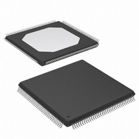
XCV50-6TQ144C Xilinx Inc, XCV50-6TQ144C Datasheet - Page 26

XCV50-6TQ144C
Manufacturer Part Number
XCV50-6TQ144C
Description
IC FPGA 2.5V C-TEMP 144-TQFP
Manufacturer
Xilinx Inc
Series
Virtex™r
Datasheet
1.XCV100-5PQ240C.pdf
(76 pages)
Specifications of XCV50-6TQ144C
Number Of Logic Elements/cells
1728
Number Of Labs/clbs
384
Total Ram Bits
32768
Number Of I /o
98
Number Of Gates
57906
Voltage - Supply
2.375 V ~ 2.625 V
Mounting Type
Surface Mount
Operating Temperature
0°C ~ 85°C
Package / Case
144-LQFP
Case
TQFP144
Dc
03+
Lead Free Status / RoHS Status
Contains lead / RoHS non-compliant
Available stocks
Company
Part Number
Manufacturer
Quantity
Price
Company:
Part Number:
XCV50-6TQ144C
Manufacturer:
XIL
Quantity:
1 238
Company:
Part Number:
XCV50-6TQ144C
Manufacturer:
XILINX
Quantity:
988
Virtex™ 2.5 V Field Programmable Gate Arrays
Virtex DC Characteristics
Absolute Maximum Ratings
Recommended Operating Conditions
Module 3 of 4
2
Notes:
1.
2.
3.
4.
Notes:
1.
2.
3.
4.
V
Symbol
V
CCINT
Symbol
V
CCO
V
V
T
T
Stresses beyond those listed under Absolute Maximum Ratings can cause permanent damage to the device. These are stress
ratings only, and functional operation of the device at these or any other conditions beyond those listed under Operating Conditions
is not implied. Exposure to Absolute Maximum Ratings conditions for extended periods of time can affect device reliability.
Power supplies can turn on in any order.
For protracted periods (e.g., longer than a day), V
For soldering guidelines and thermal considerations, see the "Device Packaging" infomation on www.xilinx.com.
Correct operation is guaranteed with a minimum V
parameters increase by 3% for each 50-mV reduction in V
At junction temperatures above those listed as Operating Conditions, delay parameters do increase. Please refer to the TRCE report.
Input and output measurement threshold is ~50% of V
Min and Max values for V
V
CCINT
V
V
CCO
REF
STG
T
IN
CC
TS
IN
J
(4)
(1)
Input Supply voltage relative to GND, T
Input Supply voltage relative to GND, T
Supply voltage relative to GND, T
Supply voltage relative to GND, T
Input signal transition time
Supply voltage relative to GND
Supply voltage relative to GND
Input Reference Voltage
Input voltage relative to GND
Voltage applied to 3-state output
Longest Supply Voltage Rise Time from 1V-2.375V
Storage temperature (ambient)
Junction temperature
CCO
are I/O Standard dependant.
(4)
(3)
Description
Description
(2)
(2)
J
J
= 0 °C to +85°C
= –40°C to +100°C
IN
CCINT
J
should not exceed V
J
= –40°C to +100°C Industrial
CC
= 0 °C to +85°C
www.xilinx.com
1-800-255-7778
of 2.375 V (Nominal V
.
CCINT
(1)
below the specified range.
Using V
Internal threshold
Plastic Packages
CCO
Commercial
Commercial
Industrial
by more than 3.6 V.
CCINT
REF
–5%). Below the minimum value, all delay
DS003-3 (v3.2) September 10, 2002
Production Product Specification
2.5 – 5%
2.5 – 5%
Min
1.4
1.4
–65 to +150
–0.5 to 3.0
–0.5 to 4.0
–0.5 to 3.6
–0.5 to 3.6
–0.5 to 5.5
–0.5 to 5.5
+125
50
2.5 + 5%
2.5 + 5%
Max
250
3.6
3.6
Units
Units
ms
°C
°C
V
V
V
V
V
V
ns
V
V
V
V
R


