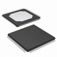
XCV50-6TQ144C Xilinx Inc, XCV50-6TQ144C Datasheet - Page 12

XCV50-6TQ144C
Manufacturer Part Number
XCV50-6TQ144C
Description
IC FPGA 2.5V C-TEMP 144-TQFP
Manufacturer
Xilinx Inc
Series
Virtex™r
Datasheet
1.XCV100-5PQ240C.pdf
(76 pages)
Specifications of XCV50-6TQ144C
Number Of Logic Elements/cells
1728
Number Of Labs/clbs
384
Total Ram Bits
32768
Number Of I /o
98
Number Of Gates
57906
Voltage - Supply
2.375 V ~ 2.625 V
Mounting Type
Surface Mount
Operating Temperature
0°C ~ 85°C
Package / Case
144-LQFP
Case
TQFP144
Dc
03+
Lead Free Status / RoHS Status
Contains lead / RoHS non-compliant
Available stocks
Company
Part Number
Manufacturer
Quantity
Price
Company:
Part Number:
XCV50-6TQ144C
Manufacturer:
XIL
Quantity:
1 238
Company:
Part Number:
XCV50-6TQ144C
Manufacturer:
XILINX
Quantity:
988
Virtex™ 2.5 V Field Programmable Gate Arrays
Four dedicated clock pads are provided, one adjacent to
each of the global buffers. The input to the global buffer is
Delay-Locked Loop (DLL)
Associated with each global clock input buffer is a fully digi-
tal Delay-Locked Loop (DLL) that can eliminate skew
between the clock input pad and internal clock-input pins
throughout the device. Each DLL can drive two global clock
networks.The DLL monitors the input clock and the distrib-
uted clock, and automatically adjusts a clock delay element.
Clock edges reach internal flip-flops one to four clock peri-
ods after they arrive at the input. This closed-loop system
effectively eliminates clock-distribution delay by ensuring
that clock edges arrive at internal flip-flops in synchronism
with clock edges arriving at the input.
In addition to eliminating clock-distribution delay, the DLL
provides advanced control of multiple clock domains. The
DLL provides four quadrature phases of the source clock,
can double the clock, or divide the clock by 1.5, 2, 2.5, 3, 4,
5, 8, or 16.
The DLL also operates as a clock mirror. By driving the out-
put from a DLL off-chip and then back on again, the DLL can
be used to de-skew a board level clock among multiple Vir-
tex devices.
In order to guarantee that the system clock is operating cor-
rectly prior to the FPGA starting up after configuration, the
DLL can delay the completion of the configuration process
until after it has achieved lock.
See DLL Timing
quency range information.
Module 2 of 4
8
Parameters, page 21
Global Clock Rows
Figure 9: Global Clock Distribution Network
of Module 3, for fre-
GCLKBUF3
GCLKPAD3
GCLKBUF1
GCLKPAD1
www.xilinx.com
1-800-255-7778
GCLKPAD2
GCLKBUF2
GCLKBUF0
selected either from these pads or from signals in the gen-
eral purpose routing.
GCLKPAD0
Boundary Scan
Virtex devices support all the mandatory boundary-scan
instructions specified in the IEEE standard 1149.1. A Test
Access Port (TAP) and registers are provided that implement
the EXTEST, INTEST, SAMPLE/PRELOAD, BYPASS,
IDCODE, USERCODE, and HIGHZ instructions. The TAP
also supports two internal scan chains and configura-
tion/readback of the device.The TAP uses dedicated package
pins that always operate using LVTTL. For TDO to operate
using LVTTL, the V
wise, TDO switches rail-to-rail between ground and V
Boundary-scan operation is independent of individual IOB
configurations, and unaffected by package type. All IOBs,
including un-bonded ones, are treated as independent
3-state bidirectional pins in a single scan chain. Retention of
the bidirectional test capability after configuration facilitates
the testing of external interconnections, provided the user
design or application is turned off.
Table 5
Virtex FPGAs. Internal signals can be captured during
EXTEST by connecting them to un-bonded or unused IOBs.
They can also be connected to the unused outputs of IOBs
defined as unidirectional input pins.
Before the device is configured, all instructions except
USER1 and USER2 are available. After configuration, all
instructions are available. During configuration, it is recom-
mended that those operations using the boundary-scan
register (SAMPLE/PRELOAD, INTEST, EXTEST) not be
performed.
lists the boundary-scan instructions supported in
gclkbu_2.eps
Global Clock Column
CCO
Global Clock Spine
for Bank 2 should be 3.3 V. Other-
DS003-2 (v2.8.1) December 9, 2002
Product Specification
CCO
.
R


